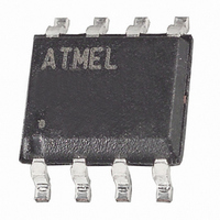
ATTINY85-20SU Atmel, ATTINY85-20SU Datasheet - Page 12

ATTINY85-20SU
Manufacturer Part Number
ATTINY85-20SU
Description
IC AVR MCU 8K 20MHZ 8SOIC
Manufacturer
Atmel
Series
AVR® ATtinyr
Specifications of ATTINY85-20SU
Core Processor
AVR
Core Size
8-Bit
Speed
20MHz
Connectivity
USI
Peripherals
Brown-out Detect/Reset, POR, PWM, WDT
Number Of I /o
6
Program Memory Size
8KB (4K x 16)
Program Memory Type
FLASH
Eeprom Size
512 x 8
Ram Size
512 x 8
Voltage - Supply (vcc/vdd)
2.7 V ~ 5.5 V
Data Converters
A/D 4x10b
Oscillator Type
Internal
Operating Temperature
-40°C ~ 85°C
Package / Case
8-SOIC (5.3mm Width), 8-SOP, 8-SOEIAJ
Processor Series
ATTINY8x
Core
AVR8
Data Bus Width
8 bit
Data Ram Size
512 B
Interface Type
USI
Maximum Clock Frequency
20 MHz
Number Of Programmable I/os
6
Number Of Timers
2
Operating Supply Voltage
2.7 V to 5.5 V
Maximum Operating Temperature
+ 85 C
Mounting Style
SMD/SMT
3rd Party Development Tools
EWAVR, EWAVR-BL
Development Tools By Supplier
ATAVRDRAGON, ATSTK500, ATSTK600, ATAVRISP2, ATAVRONEKIT
Minimum Operating Temperature
- 40 C
On-chip Adc
4-ch x 10-bit
For Use With
ATSTK600-DIP40 - STK600 SOCKET/ADAPTER 40-PDIPATAVRBC100 - REF DESIGN KIT BATTERY CHARGER770-1007 - ISP 4PORT ATMEL AVR MCU SPI/JTAG770-1004 - ISP 4PORT FOR ATMEL AVR MCU SPIATAVRDRAGON - KIT DRAGON 32KB FLASH MEM AVRATAVRISP2 - PROGRAMMER AVR IN SYSTEM
Lead Free Status / RoHS Status
Lead free / RoHS Compliant
Available stocks
Company
Part Number
Manufacturer
Quantity
Price
Part Number:
ATTINY85-20SU
Manufacturer:
ATMEL/爱特梅尔
Quantity:
20 000
- Current page: 12 of 236
- Download datasheet (5Mb)
4.7
4.8
12
Instruction Execution Timing
Reset and Interrupt Handling
ATtiny25/45/85
This section describes the general access timing concepts for instruction execution. The AVR
CPU is driven by the CPU clock clk
chip. No internal clock division is used.
Figure 4-4
vard architecture and the fast access Register File concept. This is the basic pipelining concept
to obtain up to 1 MIPS per MHz with the corresponding unique results for functions per cost,
functions per clocks, and functions per power-unit.
Figure 4-4.
Figure 4-5
operation using two register operands is executed, and the result is stored back to the destina-
tion register.
Figure 4-5.
The AVR provides several different interrupt sources. These interrupts and the separate Reset
Vector each have a separate Program Vector in the Program memory space. All interrupts are
assigned individual enable bits which must be written logic one together with the Global Interrupt
Enable bit in the Status Register in order to enable the interrupt.
The lowest addresses in the Program memory space are by default defined as the Reset and
Interrupt Vectors. The complete list of vectors is shown in
determines the priority levels of the different interrupts. The lower the address the higher is the
priority level. RESET has the highest priority, and next is INT0 – the External Interrupt Request
0.
Register Operands Fetch
2nd Instruction Execute
3rd Instruction Execute
1st Instruction Execute
ALU Operation Execute
2nd Instruction Fetch
3rd Instruction Fetch
4th Instruction Fetch
1st Instruction Fetch
Total Execution Time
shows the internal timing concept for the Register File. In a single clock cycle an ALU
shows the parallel instruction fetches and instruction executions enabled by the Har-
Result Write Back
The Parallel Instruction Fetches and Instruction Executions
Single Cycle ALU Operation
clk
clk
CPU
CPU
CPU
T1
T1
, directly generated from the selected clock source for the
T2
T2
“Interrupts” on page
T3
T3
50. The list also
2586M–AVR–07/10
T4
T4
Related parts for ATTINY85-20SU
Image
Part Number
Description
Manufacturer
Datasheet
Request
R

Part Number:
Description:
Manufacturer:
Atmel Corporation
Datasheet:

Part Number:
Description:
Manufacturer:
Atmel Corporation
Datasheet:

Part Number:
Description:
IC MCU AVR 8K FLASH 20MHZ 20-QFN
Manufacturer:
Atmel
Datasheet:

Part Number:
Description:
IC AVR MCU 8K 20MHZ 8DIP
Manufacturer:
Atmel
Datasheet:

Part Number:
Description:
MCU AVR 8K FLASH 15MHZ 8-SOIC
Manufacturer:
Atmel
Datasheet:

Part Number:
Description:
MCU AVR 8KB FLASH 20MHZ 8SOIC
Manufacturer:
Atmel
Datasheet:

Part Number:
Description:
IC MCU AVR 8KB FLASH 20MHZ 8SOIC
Manufacturer:
Atmel
Datasheet:

Part Number:
Description:
MCU AVR 8KB FLASH 20MHZ 20QFN
Manufacturer:
Atmel
Datasheet:

Part Number:
Description:
IC AVR MCU 8K 20MHZ 8DIP
Manufacturer:
Atmel
Datasheet:

Part Number:
Description:
IC AVR MCU 8K 20MHZ 8SOIC
Manufacturer:
Atmel
Datasheet:


