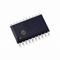
DSPIC33FJ12MC201-I/SO Microchip Technology, DSPIC33FJ12MC201-I/SO Datasheet - Page 118

DSPIC33FJ12MC201-I/SO
Manufacturer Part Number
DSPIC33FJ12MC201-I/SO
Description
IC DSPIC MCU/DSP 12K 20SOIC
Manufacturer
Microchip Technology
Series
dsPIC™ 33Fr
Datasheets
1.PIC24HJ12GP201-ISO.pdf
(84 pages)
2.DSPIC33FJ12MC201-ISO.pdf
(288 pages)
3.DSPIC33FJ12MC201-ISO.pdf
(14 pages)
4.DSPIC33FJ12MC201-IP.pdf
(284 pages)
Specifications of DSPIC33FJ12MC201-I/SO
Program Memory Type
FLASH
Program Memory Size
12KB (12K x 8)
Package / Case
20-SOIC (7.5mm Width)
Core Processor
dsPIC
Core Size
16-Bit
Speed
40 MIPs
Connectivity
I²C, IrDA, SPI, UART/USART
Peripherals
Brown-out Detect/Reset, Motor Control PWM, QEI, POR, PWM, WDT
Number Of I /o
15
Ram Size
1K x 8
Voltage - Supply (vcc/vdd)
3 V ~ 3.6 V
Data Converters
A/D 4x10b
Oscillator Type
Internal
Operating Temperature
-40°C ~ 85°C
Product
DSCs
Data Bus Width
16 bit
Processor Series
DSPIC33F
Core
dsPIC
Maximum Clock Frequency
40 MHz
Number Of Programmable I/os
15
Data Ram Size
1 KB
Maximum Operating Temperature
+ 85 C
Mounting Style
SMD/SMT
3rd Party Development Tools
52713-733, 52714-737, 53276-922, EWDSPIC
Development Tools By Supplier
PG164130, DV164035, DV244005, DV164005, PG164120, DM240001, DV164033
Minimum Operating Temperature
- 40 C
Lead Free Status / RoHS Status
Lead free / RoHS Compliant
For Use With
DV164033 - KIT START EXPLORER 16 MPLAB ICD2DM240001 - BOARD DEMO PIC24/DSPIC33/PIC32
Eeprom Size
-
Lead Free Status / Rohs Status
Lead free / RoHS Compliant
- PIC24HJ12GP201-ISO PDF datasheet
- DSPIC33FJ12MC201-ISO PDF datasheet #2
- DSPIC33FJ12MC201-ISO PDF datasheet #3
- DSPIC33FJ12MC201-IP PDF datasheet #4
- Current page: 118 of 288
- Download datasheet (5Mb)
dsPIC33FJ12MC201/202
10.1.1
In addition to the PORT, LAT, and TRIS registers for
data control, some port pins can also be individually
configured for either digital or open-drain output. This
is controlled by the Open-Drain Control register,
ODCx, associated with each port. Setting any of the
bits configures the corresponding pin to act as an
open-drain output.
The open-drain feature allows the generation of
outputs higher than V
digital-only pins by using external pull-up resistors.
The maximum open-drain voltage allowed is the same
as the maximum V
See “Pin Diagrams” for the available pins and their
functionality.
10.2
The AD1PCFG and TRIS registers control the opera-
tion of the analog-to-digital (A/D) port pins. The port
pins that are to function as analog inputs must have
their corresponding TRIS bit set (input). If the TRIS bit
is cleared (output), the digital output level (V
will be converted.
The AD1PCFGL register has a default value of 0x0000;
therefore, all pins that share ANx functions are analog
(not digital) by default.
When the PORT register is read, all pins configured as
analog input channels will read as cleared (a low level).
Pins configured as digital inputs will not convert an
analog input. Analog levels on any pin defined as a
digital input (including the ANx pins) can cause the
input buffer to consume current that exceeds the
device specifications.
10.2.1
One instruction cycle is required between a port
direction change or port write operation and a read
operation of the same port. Typically this instruction
would be an NOP. An demonstration is shown in
Example 10-1.
EXAMPLE 10-1:
DS70265D-page 116
MOV
MOV
NOP
btss
0xFF00, W0
W0, TRISBB
PORTB, #13
Configuring Analog Port Pins
OPEN-DRAIN CONFIGURATION
I/O PORT WRITE/READ TIMING
IH
specification.
PORT WRITE/READ EXAMPLE
DD
(e.g., 5V) on any desired
; Configure PORTB<15:8> as inputs
; and PORTB<7:0> as outputs
; Delay 1 cycle
; Next Instruction
OH
or V
Preliminary
OL
)
10.3
The input change notification function of the I/O ports
allows the dsPIC33FJ12MC201/202 devices to gener-
ate interrupt requests to the processor in response to a
change-of-state on selected input pins. This feature
can detect input change-of-states even in Sleep mode,
when the clocks are disabled. Depending on the device
pin count, up to 21 external signals (CNx pin) can be
selected (enabled) for generating an interrupt request
on a change-of-state.
Four control registers are associated with the CN mod-
ule. The CNEN1 and CNEN2 registers contain the
interrupt enable control bits for each of the CN input
pins. Setting any of these bits enables a CN interrupt
for the corresponding pins.
Each CN pin also has a weak pull-up connected to it.
The pull-ups act as a current source connected to the
pin, and eliminate the need for external resistors when
push-button or keypad devices are connected. The
pull-ups are enabled separately using the CNPU1 and
CNPU2 registers, which contain the control bits for
each of the CN pins. Setting any of the control bits
enables the weak pull-ups for the corresponding pins.
Note:
Input Change Notification
Pull-ups on change notification pins
should always be disabled when the port
pin is configured as a digital output.
© 2009 Microchip Technology Inc.
Related parts for DSPIC33FJ12MC201-I/SO
Image
Part Number
Description
Manufacturer
Datasheet
Request
R

Part Number:
Description:
IC, DSC, 16BIT, 12KB, 40MHZ, 3.6V, DIP28
Manufacturer:
Microchip Technology
Datasheet:

Part Number:
Description:
Manufacturer:
Microchip Technology Inc.
Datasheet:

Part Number:
Description:
Manufacturer:
Microchip Technology Inc.
Datasheet:

Part Number:
Description:
Manufacturer:
Microchip Technology Inc.
Datasheet:

Part Number:
Description:
Manufacturer:
Microchip Technology Inc.
Datasheet:

Part Number:
Description:
Manufacturer:
Microchip Technology Inc.
Datasheet:

Part Number:
Description:
Manufacturer:
Microchip Technology Inc.
Datasheet:

Part Number:
Description:
Manufacturer:
Microchip Technology Inc.
Datasheet:

Part Number:
Description:
Manufacturer:
Microchip Technology Inc.
Datasheet:


