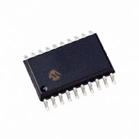
DSPIC33FJ12MC201-I/SO Microchip Technology, DSPIC33FJ12MC201-I/SO Datasheet - Page 274

DSPIC33FJ12MC201-I/SO
Manufacturer Part Number
DSPIC33FJ12MC201-I/SO
Description
IC DSPIC MCU/DSP 12K 20SOIC
Manufacturer
Microchip Technology
Series
dsPIC™ 33Fr
Datasheets
1.PIC24HJ12GP201-ISO.pdf
(84 pages)
2.DSPIC33FJ12MC201-ISO.pdf
(288 pages)
3.DSPIC33FJ12MC201-ISO.pdf
(14 pages)
4.DSPIC33FJ12MC201-IP.pdf
(284 pages)
Specifications of DSPIC33FJ12MC201-I/SO
Program Memory Type
FLASH
Program Memory Size
12KB (12K x 8)
Package / Case
20-SOIC (7.5mm Width)
Core Processor
dsPIC
Core Size
16-Bit
Speed
40 MIPs
Connectivity
I²C, IrDA, SPI, UART/USART
Peripherals
Brown-out Detect/Reset, Motor Control PWM, QEI, POR, PWM, WDT
Number Of I /o
15
Ram Size
1K x 8
Voltage - Supply (vcc/vdd)
3 V ~ 3.6 V
Data Converters
A/D 4x10b
Oscillator Type
Internal
Operating Temperature
-40°C ~ 85°C
Product
DSCs
Data Bus Width
16 bit
Processor Series
DSPIC33F
Core
dsPIC
Maximum Clock Frequency
40 MHz
Number Of Programmable I/os
15
Data Ram Size
1 KB
Maximum Operating Temperature
+ 85 C
Mounting Style
SMD/SMT
3rd Party Development Tools
52713-733, 52714-737, 53276-922, EWDSPIC
Development Tools By Supplier
PG164130, DV164035, DV244005, DV164005, PG164120, DM240001, DV164033
Minimum Operating Temperature
- 40 C
Lead Free Status / RoHS Status
Lead free / RoHS Compliant
For Use With
DV164033 - KIT START EXPLORER 16 MPLAB ICD2DM240001 - BOARD DEMO PIC24/DSPIC33/PIC32
Eeprom Size
-
Lead Free Status / Rohs Status
Lead free / RoHS Compliant
- PIC24HJ12GP201-ISO PDF datasheet
- DSPIC33FJ12MC201-ISO PDF datasheet #2
- DSPIC33FJ12MC201-ISO PDF datasheet #3
- DSPIC33FJ12MC201-IP PDF datasheet #4
- Current page: 274 of 288
- Download datasheet (5Mb)
dsPIC33FJ12MC201/202
Revision C (June 2008)
This revision includes minor typographical and
formatting changes throughout the data sheet text.
The major changes are referenced by their respective
section in the following table.
TABLE 25-1:
DS70265D-page 272
“High-Performance, 16-bit
Digital Signal Controllers”
Section 1.0 “Device Overview”
Section 3.0 “Memory
Organization”
Section 4.0 “Flash Program
Memory”
Section 5.0 “Resets”
Section 7.0 “Oscillator
Configuration”
Section 8.0 “Power-Saving
Features”
Section Name
MAJOR SECTION UPDATES
Added SSOP to list of available 28-pin packages (see “Packaging:” and
Table 1).
Added External Interrupts column to Remappable Peripherals in the Controller
Families table and Note 2 (see Table 1).
Added Note 1 to all pin diagrams, which references RPn pin usage by
remappable peripherals (see “Pin Diagrams”).
Changed Capture Input pin names from IC0-IC1 to IC1-IC2 and updated
description for AV
Added SFR definitions (ACCAL, ACCAH, ACCAU, ACCBL, ACCBH, and
ACCBU) to the CPU Core Register Map (see Table 3-1).
Updated Reset values for the following SFRs: IPC0, IPC2-IPC7, IPC16, and
INTTREG (see Table 3-4).
Updated all SFR names in QEI1 Register Map (see Table 3-11).
The following changes were made to the ADC1 Register Maps:
• Updated the bit range for AD1CON3 from ADCS<5:0> to ADCS<7:0>)
• Added Bit 6 (PCFG7) and Bit 7 (PCFG6) names to AD1PCFGL (Table 3-15).
• Added Bit 6 (CSS7) and Bit 7 (CSS6) names to AD1CSSL (see Table 3-15).
• Changed Bit 5 and Bit 4 in AD1CSSL to unimplemented (see Table 3-15).
Updated the Reset value for CLKDIV in the System Control Register Map
(see Table 3-23).
Updated Section 4.3 “Programming Operations” with programming time
formula.
Entire section was replaced to maintain consistency with other dsPIC33F data
sheets.
Removed the first sentence of the third clock source item (External Clock) in
Section 7.1.1 “System Clock sources”
Updated the default bit values for DOZE and FRCDIV in the Clock Divisor
Register (see Register 7-2).
Added the center frequency in the OSCTUN register for the FRC Tuning bits
(TUN<5:0>) value 011111 and updated the center frequency for bits value
011110 (see Register 7-4)
Added the following three registers:
• PMD1: Peripheral Module Disable Control Register 1
• PMD2: Peripheral Module Disable Control Register 2
• PMD3: Peripheral Module Disable Control Register 3
(see Table 3-15 and Table 3-16).
Preliminary
DD
(see Table 1-1).
Update Description
© 2009 Microchip Technology Inc.
Related parts for DSPIC33FJ12MC201-I/SO
Image
Part Number
Description
Manufacturer
Datasheet
Request
R

Part Number:
Description:
IC, DSC, 16BIT, 12KB, 40MHZ, 3.6V, DIP28
Manufacturer:
Microchip Technology
Datasheet:

Part Number:
Description:
Manufacturer:
Microchip Technology Inc.
Datasheet:

Part Number:
Description:
Manufacturer:
Microchip Technology Inc.
Datasheet:

Part Number:
Description:
Manufacturer:
Microchip Technology Inc.
Datasheet:

Part Number:
Description:
Manufacturer:
Microchip Technology Inc.
Datasheet:

Part Number:
Description:
Manufacturer:
Microchip Technology Inc.
Datasheet:

Part Number:
Description:
Manufacturer:
Microchip Technology Inc.
Datasheet:

Part Number:
Description:
Manufacturer:
Microchip Technology Inc.
Datasheet:

Part Number:
Description:
Manufacturer:
Microchip Technology Inc.
Datasheet:


