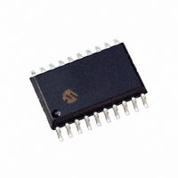
DSPIC33FJ12MC201-I/SO Microchip Technology, DSPIC33FJ12MC201-I/SO Datasheet - Page 65

DSPIC33FJ12MC201-I/SO
Manufacturer Part Number
DSPIC33FJ12MC201-I/SO
Description
IC DSPIC MCU/DSP 12K 20SOIC
Manufacturer
Microchip Technology
Series
dsPIC™ 33Fr
Datasheets
1.PIC24HJ12GP201-ISO.pdf
(84 pages)
2.DSPIC33FJ12MC201-ISO.pdf
(288 pages)
3.DSPIC33FJ12MC201-ISO.pdf
(14 pages)
4.DSPIC33FJ12MC201-IP.pdf
(284 pages)
Specifications of DSPIC33FJ12MC201-I/SO
Program Memory Type
FLASH
Program Memory Size
12KB (12K x 8)
Package / Case
20-SOIC (7.5mm Width)
Core Processor
dsPIC
Core Size
16-Bit
Speed
40 MIPs
Connectivity
I²C, IrDA, SPI, UART/USART
Peripherals
Brown-out Detect/Reset, Motor Control PWM, QEI, POR, PWM, WDT
Number Of I /o
15
Ram Size
1K x 8
Voltage - Supply (vcc/vdd)
3 V ~ 3.6 V
Data Converters
A/D 4x10b
Oscillator Type
Internal
Operating Temperature
-40°C ~ 85°C
Product
DSCs
Data Bus Width
16 bit
Processor Series
DSPIC33F
Core
dsPIC
Maximum Clock Frequency
40 MHz
Number Of Programmable I/os
15
Data Ram Size
1 KB
Maximum Operating Temperature
+ 85 C
Mounting Style
SMD/SMT
3rd Party Development Tools
52713-733, 52714-737, 53276-922, EWDSPIC
Development Tools By Supplier
PG164130, DV164035, DV244005, DV164005, PG164120, DM240001, DV164033
Minimum Operating Temperature
- 40 C
Lead Free Status / RoHS Status
Lead free / RoHS Compliant
For Use With
DV164033 - KIT START EXPLORER 16 MPLAB ICD2DM240001 - BOARD DEMO PIC24/DSPIC33/PIC32
Eeprom Size
-
Lead Free Status / Rohs Status
Lead free / RoHS Compliant
- PIC24HJ12GP201-ISO PDF datasheet
- DSPIC33FJ12MC201-ISO PDF datasheet #2
- DSPIC33FJ12MC201-ISO PDF datasheet #3
- DSPIC33FJ12MC201-IP PDF datasheet #4
- Current page: 65 of 288
- Download datasheet (5Mb)
FIGURE 6-2:
TABLE 6-2:
© 2009 Microchip Technology Inc.
V
T
V
T
T
T
Symbol
POR
BOR
PWRT
FSCM
POR
BOR
Oscillator Clock
Device Status
1.
2.
3.
4.
5.
6.
POR Reset
BOR Reset
SYSRST
POR threshold
POR extension time 30 μs maximum
BOR threshold
BOR extension time 100 μs maximum
Programmable
power-up time delay
Fail-safe Clock
Monitor Delay
FSCM
POR Reset: A POR circuit holds the device in Reset when the power supply is turned on. The POR circuit is active until V
the V
BOR Reset: The on-chip voltage regulator has a BOR circuit that keeps the device in Reset until V
and the delay T
PWRT Timer: The programmable power-up timer continues to hold the processor in Reset for a specific period of time (T
after a BOR. The delay T
ation. After the delay T
erating clock cycles.
Oscillator Delay: The total delay for the clock to be ready for various clock source selections are given in Table 6-1. Refer to
Section 8.0 “Oscillator Configuration” for more information.
When the oscillator clock is ready, the processor begins execution from location 0x000000. The user application programs a GOTO
instruction at the Reset address, which redirects program execution to the appropriate start-up routine.
The Fail-safe clock monitor (FSCM), if enabled, begins to monitor the system clock when the system clock is ready and the delay
T
FSCM
V
DD
Parameter
POR
elapsed.
OSCILLATOR DELAY
threshold and the delay T
1
SYSTEM RESET TIMING
BOR
has elapsed. The delay T
2
PWRT
PWRT
1.8V nominal
2.5V nominal
0-128 ms nominal
900 μs maximum
T
V
has elapsed, the SYSRST becomes inactive, which in turn enables the selected oscillator to start gen-
POR
POR
ensures that the system power supplies have stabilized at the appropriate level for full-speed oper-
POR
Value
has elapsed.
BOR
Preliminary
Vbor
ensures the voltage regulator output becomes stable.
V
BOR
dsPIC33FJ12MC201/202
T
PWRT
T
3
BOR
Reset
Time
Note:
T
OSCD
When the device exits the Reset condi-
tion (begins normal operation), the
device operating parameters (voltage,
frequency, temperature, etc.) must be
within their operating ranges, otherwise
the device may not function correctly.
The user application must ensure that
the delay between the time power is
first applied, and the time SYSRST
becomes inactive, is long enough to get
all
specification.
T
OST
4
operating
DD
T
crosses the V
LOCK
parameters
DS70265D-page 63
5
BOR
6
Run
DD
threshold
T
crosses
FSCM
PWRT
within
)
Related parts for DSPIC33FJ12MC201-I/SO
Image
Part Number
Description
Manufacturer
Datasheet
Request
R

Part Number:
Description:
IC, DSC, 16BIT, 12KB, 40MHZ, 3.6V, DIP28
Manufacturer:
Microchip Technology
Datasheet:

Part Number:
Description:
Manufacturer:
Microchip Technology Inc.
Datasheet:

Part Number:
Description:
Manufacturer:
Microchip Technology Inc.
Datasheet:

Part Number:
Description:
Manufacturer:
Microchip Technology Inc.
Datasheet:

Part Number:
Description:
Manufacturer:
Microchip Technology Inc.
Datasheet:

Part Number:
Description:
Manufacturer:
Microchip Technology Inc.
Datasheet:

Part Number:
Description:
Manufacturer:
Microchip Technology Inc.
Datasheet:

Part Number:
Description:
Manufacturer:
Microchip Technology Inc.
Datasheet:

Part Number:
Description:
Manufacturer:
Microchip Technology Inc.
Datasheet:


