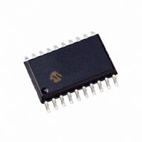
DSPIC33FJ12MC201-I/SO Microchip Technology, DSPIC33FJ12MC201-I/SO Datasheet - Page 209

DSPIC33FJ12MC201-I/SO
Manufacturer Part Number
DSPIC33FJ12MC201-I/SO
Description
IC DSPIC MCU/DSP 12K 20SOIC
Manufacturer
Microchip Technology
Series
dsPIC™ 33Fr
Datasheets
1.PIC24HJ12GP201-ISO.pdf
(84 pages)
2.DSPIC33FJ12MC201-ISO.pdf
(288 pages)
3.DSPIC33FJ12MC201-ISO.pdf
(14 pages)
4.DSPIC33FJ12MC201-IP.pdf
(284 pages)
Specifications of DSPIC33FJ12MC201-I/SO
Program Memory Type
FLASH
Program Memory Size
12KB (12K x 8)
Package / Case
20-SOIC (7.5mm Width)
Core Processor
dsPIC
Core Size
16-Bit
Speed
40 MIPs
Connectivity
I²C, IrDA, SPI, UART/USART
Peripherals
Brown-out Detect/Reset, Motor Control PWM, QEI, POR, PWM, WDT
Number Of I /o
15
Ram Size
1K x 8
Voltage - Supply (vcc/vdd)
3 V ~ 3.6 V
Data Converters
A/D 4x10b
Oscillator Type
Internal
Operating Temperature
-40°C ~ 85°C
Product
DSCs
Data Bus Width
16 bit
Processor Series
DSPIC33F
Core
dsPIC
Maximum Clock Frequency
40 MHz
Number Of Programmable I/os
15
Data Ram Size
1 KB
Maximum Operating Temperature
+ 85 C
Mounting Style
SMD/SMT
3rd Party Development Tools
52713-733, 52714-737, 53276-922, EWDSPIC
Development Tools By Supplier
PG164130, DV164035, DV244005, DV164005, PG164120, DM240001, DV164033
Minimum Operating Temperature
- 40 C
Lead Free Status / RoHS Status
Lead free / RoHS Compliant
For Use With
DV164033 - KIT START EXPLORER 16 MPLAB ICD2DM240001 - BOARD DEMO PIC24/DSPIC33/PIC32
Eeprom Size
-
Lead Free Status / Rohs Status
Lead free / RoHS Compliant
- PIC24HJ12GP201-ISO PDF datasheet
- DSPIC33FJ12MC201-ISO PDF datasheet #2
- DSPIC33FJ12MC201-ISO PDF datasheet #3
- DSPIC33FJ12MC201-IP PDF datasheet #4
- Current page: 209 of 288
- Download datasheet (5Mb)
21.5
dsPIC33FJ12MC201/202 devices implement a JTAG
interface, which supports boundary scan device test-
ing, as well as in-circuit programming. Detailed infor-
mation on this interface will be provided in future
revisions of the document.
21.6
The dsPIC33FJ12MC201/202 devices can be serially
programmed while in the end application circuit. This is
done with two lines for clock and data and three other
lines for power, ground and the programming
sequence. Serial programming allows customers to
manufacture boards with unprogrammed devices and
then program the digital signal controller just before
shipping the product. Serial programming also allows
the most recent firmware or a custom firmware to be
programmed. Refer to the dsPIC33F/PIC24H Flash
Programming Specification (DS70152) for details
about In-Circuit Serial Programming (ICSP).
Any of the three pairs of programming clock/data pins
can be used:
• PGEC1 and PGED1
• PGEC2 and PGED2
• PGEC3 and PGED3
21.7
When MPLAB
circuit debugging functionality is enabled. This function
allows simple debugging functions when used with
MPLAB IDE. Debugging functionality is controlled
through the PGECx (Emulation/Debug Clock) and
PGEDx (Emulation/Debug Data) pin functions.
Any of the three pairs of debugging clock/data pins can
be used:
• PGEC1 and PGED1
• PGEC2 and PGED2
• PGEC3 and PGED3
To use the in-circuit debugger function of the device,
the design must implement ICSP connections to
MCLR, V
addition, when the feature is enabled, some of the
resources are not available for general use. These
resources include the first 80 bytes of data RAM and
two I/O pins.
© 2009 Microchip Technology Inc.
JTAG Interface
In-Circuit Debugger
DD
In-Circuit Serial Programming
, V
®
SS
ICD 2 is selected as a debugger, the in-
, and the PGECx/PGEDx pin pair. In
Preliminary
dsPIC33FJ12MC201/202
21.8
The
intermediate implementation of CodeGuard Security.
CodeGuard Security enables multiple parties to
securely share resources (memory, interrupts and
peripherals) on a single chip. This feature helps protect
individual Intellectual Property in collaborative system
designs.
When coupled with software encryption libraries,
CodeGuard Security can be used to securely update
Flash even when multiple IPs reside on the single chip.
The code protection features vary depending on the
actual dsPIC33F implemented. The following sections
provide an overview of these features.
Secure
implemented in dsPIC33FJ12MC201/202 devices.
TABLE 21-3:
BSS<2:0> = x11
BSS<2:0> = x10
BSS<2:0> = x01
BSS<2:0> = x00
Note:
CONFIG BITS
dsPIC33FJ12MC201/202
1792
256
768
0K
Code Protection and
CodeGuard™ Security
segment
Refer to Section 23. “CodeGuard™
Security” (DS70199) of the “dsPIC33F
Family Reference Manual” for further
information on usage, configuration and
operation of CodeGuard Security.
CODE FLASH SECURITY
SEGMENT SIZES FOR
12 KBYTE DEVICES
and
GS = 3840 IW
GS = 3584 IW
GS = 3072 IW
BS = 1792 IW
GS = 2048 IW
VS = 256 IW
VS = 256 IW
BS = 256 IW
VS = 256 IW
BS = 768 IW
VS = 256 IW
RAM
devices
protection
DS70265D-page 207
000000h
000200h
000400h
000800h
001000h
000000h
000200h
000400h
000800h
001000h
000000h
000200h
000400h
000800h
001000h
000000h
000200h
000400h
000800h
001000h
0001FEh
0003FEh
0007FEh
000FFEh
001FFEh
0001FEh
0003FEh
0007FEh
000FFEh
001FFEh
0001FEh
0003FEh
0007FEh
000FFEh
001FFEh
0001FEh
0003FEh
0007FEh
000FFEh
001FFEh
offer
is
the
not
Related parts for DSPIC33FJ12MC201-I/SO
Image
Part Number
Description
Manufacturer
Datasheet
Request
R

Part Number:
Description:
IC, DSC, 16BIT, 12KB, 40MHZ, 3.6V, DIP28
Manufacturer:
Microchip Technology
Datasheet:

Part Number:
Description:
Manufacturer:
Microchip Technology Inc.
Datasheet:

Part Number:
Description:
Manufacturer:
Microchip Technology Inc.
Datasheet:

Part Number:
Description:
Manufacturer:
Microchip Technology Inc.
Datasheet:

Part Number:
Description:
Manufacturer:
Microchip Technology Inc.
Datasheet:

Part Number:
Description:
Manufacturer:
Microchip Technology Inc.
Datasheet:

Part Number:
Description:
Manufacturer:
Microchip Technology Inc.
Datasheet:

Part Number:
Description:
Manufacturer:
Microchip Technology Inc.
Datasheet:

Part Number:
Description:
Manufacturer:
Microchip Technology Inc.
Datasheet:


