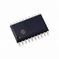
DSPIC33FJ12MC201-I/SO Microchip Technology, DSPIC33FJ12MC201-I/SO Datasheet - Page 67

DSPIC33FJ12MC201-I/SO
Manufacturer Part Number
DSPIC33FJ12MC201-I/SO
Description
IC DSPIC MCU/DSP 12K 20SOIC
Manufacturer
Microchip Technology
Series
dsPIC™ 33Fr
Datasheets
1.PIC24HJ12GP201-ISO.pdf
(84 pages)
2.DSPIC33FJ12MC201-ISO.pdf
(288 pages)
3.DSPIC33FJ12MC201-ISO.pdf
(14 pages)
4.DSPIC33FJ12MC201-IP.pdf
(284 pages)
Specifications of DSPIC33FJ12MC201-I/SO
Program Memory Type
FLASH
Program Memory Size
12KB (12K x 8)
Package / Case
20-SOIC (7.5mm Width)
Core Processor
dsPIC
Core Size
16-Bit
Speed
40 MIPs
Connectivity
I²C, IrDA, SPI, UART/USART
Peripherals
Brown-out Detect/Reset, Motor Control PWM, QEI, POR, PWM, WDT
Number Of I /o
15
Ram Size
1K x 8
Voltage - Supply (vcc/vdd)
3 V ~ 3.6 V
Data Converters
A/D 4x10b
Oscillator Type
Internal
Operating Temperature
-40°C ~ 85°C
Product
DSCs
Data Bus Width
16 bit
Processor Series
DSPIC33F
Core
dsPIC
Maximum Clock Frequency
40 MHz
Number Of Programmable I/os
15
Data Ram Size
1 KB
Maximum Operating Temperature
+ 85 C
Mounting Style
SMD/SMT
3rd Party Development Tools
52713-733, 52714-737, 53276-922, EWDSPIC
Development Tools By Supplier
PG164130, DV164035, DV244005, DV164005, PG164120, DM240001, DV164033
Minimum Operating Temperature
- 40 C
Lead Free Status / RoHS Status
Lead free / RoHS Compliant
For Use With
DV164033 - KIT START EXPLORER 16 MPLAB ICD2DM240001 - BOARD DEMO PIC24/DSPIC33/PIC32
Eeprom Size
-
Lead Free Status / Rohs Status
Lead free / RoHS Compliant
- PIC24HJ12GP201-ISO PDF datasheet
- DSPIC33FJ12MC201-ISO PDF datasheet #2
- DSPIC33FJ12MC201-ISO PDF datasheet #3
- DSPIC33FJ12MC201-IP PDF datasheet #4
- Current page: 67 of 288
- Download datasheet (5Mb)
6.4
The external Reset is generated by driving the MCLR
pin low. The MCLR pin is a Schmitt trigger input with an
additional glitch filter. Reset pulses that are longer than
the minimum pulse width will generate a Reset. Refer
to Section 24.0 “Electrical Characteristics” for
minimum pulse width specifications. The External
Reset (MCLR) Pin (EXTR) bit in the Reset Control
(RCON) register is set to indicate the MCLR Reset.
6.4.0.1
Many systems have external supervisory circuits that
generate Reset signals to Reset multiple devices in the
system. This external Reset signal can be directly con-
nected to the MCLR pin to Reset the device when the
rest of system is Reset.
6.4.0.2
When using the internal power supervisory circuit to
Reset the device, the external Reset pin (MCLR)
should be tied directly or resistively to V
the MCLR pin will not be used to generate a Reset. The
external Reset pin (MCLR) does not have an internal
pull-up and must not be left unconnected.
6.5
Whenever the RESET instruction is executed, the
device will assert SYSRST, placing the device in a
special Reset state. This Reset state will not re-
initialize the clock. The clock source in effect prior to the
RESET instruction will remain. SYSRST is released at
the next instruction cycle, and the Reset vector fetch
will commence.
The Software Reset (Instruction) Flag (SWR) bit in the
Reset Control (RCON<6>) register is set to indicate
the software Reset.
6.6
Whenever a Watchdog Time-out occurs, the device
will asynchronously assert SYSRST. The clock source
will remain unchanged. A WDT time-out during Sleep
or Idle mode will wake-up the processor, but will not
reset the processor.
The Watchdog Timer Time-out Flag (WDTO) bit in the
Reset Control (RCON<4>) register is set to indicate
the
“Watchdog Timer (WDT)” for more information on
Watchdog Reset.
© 2009 Microchip Technology Inc.
Watchdog
External Reset (EXTR)
Software RESET Instruction (SWR)
Watchdog Time-out Reset (WDTO)
EXTERNAL SUPERVISORY CIRCUIT
INTERNAL SUPERVISORY CIRCUIT
Reset.
Refer
to
DD
Section 21.4
. In this case,
Preliminary
dsPIC33FJ12MC201/202
6.7
If a lower-priority hard trap occurs while a higher-prior-
ity trap is being processed, a hard trap conflict Reset
occurs. The hard traps include exceptions of priority
level 13 through level 15, inclusive. The address error
(level 13) and oscillator error (level 14) traps fall into
this category.
The Trap Reset Flag (TRAPR) bit in the Reset Control
(RCON<15>) register is set to indicate the Trap Conflict
Reset. Refer to Section 7.0 “Interrupt Controller” for
more information on trap conflict Resets.
6.8
To maintain the integrity of the peripheral pin select
control registers, they are constantly monitored with
shadow registers in hardware. If an unexpected
change in any of the registers occur (such as cell dis-
turbances caused by ESD or other external events), a
configuration mismatch Reset occurs.
The Configuration Mismatch Flag (CM) bit in the
Reset Control (RCON<9>) register is set to indicate
the
Section 10.0 “I/O Ports” for more information on the
configuration mismatch Reset.
6.9
An illegal condition device Reset occurs due to the
following sources:
• Illegal Opcode Reset
• Uninitialized W Register Reset
• Security Reset
The Illegal Opcode or Uninitialized W Access Reset
Flag (IOPUWR) bit in the Reset Control (RCON<14>)
register is set to indicate the illegal condition device
Reset.
Note:
configuration
Trap Conflict Reset
Configuration Mismatch Reset
Illegal Condition Device Reset
The configuration mismatch feature and
associated Reset flag is not available on
all devices.
mismatch
Reset.
DS70265D-page 65
Refer
to
Related parts for DSPIC33FJ12MC201-I/SO
Image
Part Number
Description
Manufacturer
Datasheet
Request
R

Part Number:
Description:
IC, DSC, 16BIT, 12KB, 40MHZ, 3.6V, DIP28
Manufacturer:
Microchip Technology
Datasheet:

Part Number:
Description:
Manufacturer:
Microchip Technology Inc.
Datasheet:

Part Number:
Description:
Manufacturer:
Microchip Technology Inc.
Datasheet:

Part Number:
Description:
Manufacturer:
Microchip Technology Inc.
Datasheet:

Part Number:
Description:
Manufacturer:
Microchip Technology Inc.
Datasheet:

Part Number:
Description:
Manufacturer:
Microchip Technology Inc.
Datasheet:

Part Number:
Description:
Manufacturer:
Microchip Technology Inc.
Datasheet:

Part Number:
Description:
Manufacturer:
Microchip Technology Inc.
Datasheet:

Part Number:
Description:
Manufacturer:
Microchip Technology Inc.
Datasheet:


