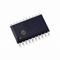
DSPIC33FJ12MC201-I/SO Microchip Technology, DSPIC33FJ12MC201-I/SO Datasheet - Page 202

DSPIC33FJ12MC201-I/SO
Manufacturer Part Number
DSPIC33FJ12MC201-I/SO
Description
IC DSPIC MCU/DSP 12K 20SOIC
Manufacturer
Microchip Technology
Series
dsPIC™ 33Fr
Datasheets
1.PIC24HJ12GP201-ISO.pdf
(84 pages)
2.DSPIC33FJ12MC201-ISO.pdf
(288 pages)
3.DSPIC33FJ12MC201-ISO.pdf
(14 pages)
4.DSPIC33FJ12MC201-IP.pdf
(284 pages)
Specifications of DSPIC33FJ12MC201-I/SO
Program Memory Type
FLASH
Program Memory Size
12KB (12K x 8)
Package / Case
20-SOIC (7.5mm Width)
Core Processor
dsPIC
Core Size
16-Bit
Speed
40 MIPs
Connectivity
I²C, IrDA, SPI, UART/USART
Peripherals
Brown-out Detect/Reset, Motor Control PWM, QEI, POR, PWM, WDT
Number Of I /o
15
Ram Size
1K x 8
Voltage - Supply (vcc/vdd)
3 V ~ 3.6 V
Data Converters
A/D 4x10b
Oscillator Type
Internal
Operating Temperature
-40°C ~ 85°C
Product
DSCs
Data Bus Width
16 bit
Processor Series
DSPIC33F
Core
dsPIC
Maximum Clock Frequency
40 MHz
Number Of Programmable I/os
15
Data Ram Size
1 KB
Maximum Operating Temperature
+ 85 C
Mounting Style
SMD/SMT
3rd Party Development Tools
52713-733, 52714-737, 53276-922, EWDSPIC
Development Tools By Supplier
PG164130, DV164035, DV244005, DV164005, PG164120, DM240001, DV164033
Minimum Operating Temperature
- 40 C
Lead Free Status / RoHS Status
Lead free / RoHS Compliant
For Use With
DV164033 - KIT START EXPLORER 16 MPLAB ICD2DM240001 - BOARD DEMO PIC24/DSPIC33/PIC32
Eeprom Size
-
Lead Free Status / Rohs Status
Lead free / RoHS Compliant
- PIC24HJ12GP201-ISO PDF datasheet
- DSPIC33FJ12MC201-ISO PDF datasheet #2
- DSPIC33FJ12MC201-ISO PDF datasheet #3
- DSPIC33FJ12MC201-IP PDF datasheet #4
- Current page: 202 of 288
- Download datasheet (5Mb)
dsPIC33FJ12MC201/202
REGISTER 20-6:
REGISTER 20-7:
DS70265D-page 200
,2
bit 15
bit 7
Legend:
R = Readable bit
-n = Value at POR
bit 15-6
bit 5-0
bit 15
bit 7
Legend:
R = Readable bit
-n = Value at POR
bit 15-6
bit 5-0
Note 1: On devices without 6 analog inputs, all AD1CSSL bits can be selected by user application. However, inputs
Note 1: On devices without 6 analog inputs, all PCFG bits are R/W by user. However, PCFG bits are ignored on
U-0
U-0
U-0
U-0
—
—
—
—
2: CSSx = ANx, where x = 0 through 5.
2: PCFGx = ANx, where x = 0 through 5.
3: PCFGx bits have no effect if the ADC module is disabled by setting ADxMD bit in the PMDx register. When
selected for scan without a corresponding input on device converts V
ports without a corresponding input on device.
the bit is set, all port pins that have been multiplexed with ANx will be in Digital mode.
Unimplemented: Read as ‘0’
CSS<5:0>: ADC Input Scan Selection bits
1 = Select ANx for input scan
0 = Skip ANx for input scan
Unimplemented: Read as ‘0’
PCFG<5:0>: ADC Port Configuration Control bits
1 = Port pin in Digital mode, port read input enabled, ADC input multiplexer connected to AV
0 = Port pin in Analog mode, port read input disabled, ADC samples pin voltage
U-0
U-0
U-0
U-0
—
—
—
—
AD1CSSL: ADC1 INPUT SCAN SELECT REGISTER LOW
AD1PCFGL: ADC1 PORT CONFIGURATION REGISTER LOW
W = Writable bit
‘1’ = Bit is set
W = Writable bit
‘1’ = Bit is set
PCFG5
R/W-0
R/W-0
CSS5
U-0
U-0
—
—
PCFG4
R/W-0
R/W-0
CSS4
Preliminary
U-0
U-0
—
—
U = Unimplemented bit, read as ‘0’
‘0’ = Bit is cleared
U = Unimplemented bit, read as ‘0’
‘0’ = Bit is cleared
PCFG3
R/W-0
R/W-0
CSS3
U-0
U-0
—
—
PCFG2
R/W-0
R/W-0
CSS2
U-0
U-0
—
—
REFL
.
© 2009 Microchip Technology Inc.
(1,2)
x = Bit is unknown
x = Bit is unknown
PCFG1
R/W-0
R/W-0
CSS1
(1,2,3)
U-0
U-0
—
—
PCFG0
R/W-0
R/W-0
CSS0
SS
U-0
U-0
—
—
bit 8
bit 0
bit 8
bit 0
Related parts for DSPIC33FJ12MC201-I/SO
Image
Part Number
Description
Manufacturer
Datasheet
Request
R

Part Number:
Description:
IC, DSC, 16BIT, 12KB, 40MHZ, 3.6V, DIP28
Manufacturer:
Microchip Technology
Datasheet:

Part Number:
Description:
Manufacturer:
Microchip Technology Inc.
Datasheet:

Part Number:
Description:
Manufacturer:
Microchip Technology Inc.
Datasheet:

Part Number:
Description:
Manufacturer:
Microchip Technology Inc.
Datasheet:

Part Number:
Description:
Manufacturer:
Microchip Technology Inc.
Datasheet:

Part Number:
Description:
Manufacturer:
Microchip Technology Inc.
Datasheet:

Part Number:
Description:
Manufacturer:
Microchip Technology Inc.
Datasheet:

Part Number:
Description:
Manufacturer:
Microchip Technology Inc.
Datasheet:

Part Number:
Description:
Manufacturer:
Microchip Technology Inc.
Datasheet:


