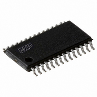
P89LPC936FDH,518 NXP Semiconductors, P89LPC936FDH,518 Datasheet - Page 10

P89LPC936FDH,518
Manufacturer Part Number
P89LPC936FDH,518
Description
IC 80C51 MCU FLASH 16K 28TSSOP
Manufacturer
NXP Semiconductors
Series
LPC900r
Datasheet
1.P89LPC936FDH518.pdf
(77 pages)
Specifications of P89LPC936FDH,518
Program Memory Type
FLASH
Program Memory Size
16KB (16K x 8)
Package / Case
28-TSSOP
Core Processor
8051
Core Size
8-Bit
Speed
18MHz
Connectivity
I²C, SPI, UART/USART
Peripherals
Brown-out Detect/Reset, LED, POR, PWM, WDT
Number Of I /o
26
Eeprom Size
512 x 8
Ram Size
768 x 8
Voltage - Supply (vcc/vdd)
2.4 V ~ 3.6 V
Data Converters
A/D 8x8b; D/A 2x8b
Oscillator Type
Internal
Operating Temperature
-40°C ~ 85°C
Processor Series
P89LPC9x
Core
80C51
Data Bus Width
8 bit
Data Ram Size
768 B
Interface Type
I2C/SPI/UART
Maximum Clock Frequency
18 MHz
Number Of Programmable I/os
26
Number Of Timers
2
Operating Supply Voltage
21 V
Maximum Operating Temperature
+ 85 C
Mounting Style
SMD/SMT
3rd Party Development Tools
PK51, CA51, A51, ULINK2
Minimum Operating Temperature
- 40 C
On-chip Adc
8-ch x 8-bit
On-chip Dac
2-ch x 8-bit
Lead Free Status / RoHS Status
Lead free / RoHS Compliant
For Use With
622-1014 - BOARD FOR LPC9XX TSSOP622-1008 - BOARD FOR LPC9103 10-HVSON622-1006 - SOCKET ADAPTER BOARDMCB900K - BOARD PROTOTYPE NXP 89LPC9EPM900K - EMULATOR/PROGRAMMER NXP P89LPC9568-4000 - DEMO BOARD SPI/I2C TO DUAL UART568-3510 - DEMO BOARD SPI/I2C TO UART622-1002 - USB IN-CIRCUIT PROG LPC9XX568-1759 - EMULATOR DEBUGGER/PROGRMMR LPC9X568-1758 - BOARD EVAL FOR LPC93X MCU FAMILY
Lead Free Status / Rohs Status
Lead free / RoHS Compliant
Other names
568-4339-2
935277841518
P89LPC936FDH-T
P89LPC936FDH-T
935277841518
P89LPC936FDH-T
P89LPC936FDH-T
NXP Semiconductors
Table 4.
[1]
P89LPC933_934_935_936
Product data sheet
Symbol
P3.0 to P3.1
P3.0/XTAL2/
CLKOUT
P3.1/XTAL1
V
V
SS
DD
Input/output for P1.0 to P1.4, P1.6, P1.7. Input for P1.5.
Pin description
Pin
TSSOP28,
PLCC28
9
8
7
21
4
HVQFN28
5
3
17
…continued
Type
I/O
O
O
I/O
I
I
I
I/O
All information provided in this document is subject to legal disclaimers.
Description
Port 3: Port 3 is a 2-bit I/O port with a user-configurable output type.
During reset Port 3 latches are configured in the input only mode with the
internal pull-up disabled. The operation of Port 3 pins as inputs and
outputs depends upon the port configuration selected. Each port pin is
configured independently. Refer to
and
All pins have Schmitt trigger inputs.
Port 3 also provides various special functions as described below:
P3.0 — Port 3 bit 0.
XTAL2 — Output from the oscillator amplifier (when a crystal oscillator
option is selected via the flash configuration.
CLKOUT — CPU clock divided by 2 when enabled via SFR bit (ENCLK -
TRIM.6). It can be used if the CPU clock is the internal RC oscillator,
watchdog oscillator or external clock input, except when XTAL1/XTAL2
are used to generate clock source for the RTC/system timer.
P3.1 — Port 3 bit 1.
XTAL1 — Input to the oscillator circuit and internal clock generator circuits
(when selected via the flash configuration). It can be a port pin if internal
RC oscillator or watchdog oscillator is used as the CPU clock source, and
if XTAL1/XTAL2 are not used to generate the clock for the RTC/system
timer.
Ground: 0 V reference.
Power supply: This is the power supply voltage for normal operation as
well as Idle and Power-down modes.
Rev. 8 — 12 January 2011
8-bit microcontroller with accelerated two-clock 80C51 core
Table 11 “Static characteristics”
P89LPC933/934/935/936
Section 8.13.1 “Port configurations”
for details.
© NXP B.V. 2011. All rights reserved.
10 of 77


