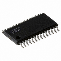
P89LPC936FDH,518 NXP Semiconductors, P89LPC936FDH,518 Datasheet - Page 54

P89LPC936FDH,518
Manufacturer Part Number
P89LPC936FDH,518
Description
IC 80C51 MCU FLASH 16K 28TSSOP
Manufacturer
NXP Semiconductors
Series
LPC900r
Datasheet
1.P89LPC936FDH518.pdf
(77 pages)
Specifications of P89LPC936FDH,518
Program Memory Type
FLASH
Program Memory Size
16KB (16K x 8)
Package / Case
28-TSSOP
Core Processor
8051
Core Size
8-Bit
Speed
18MHz
Connectivity
I²C, SPI, UART/USART
Peripherals
Brown-out Detect/Reset, LED, POR, PWM, WDT
Number Of I /o
26
Eeprom Size
512 x 8
Ram Size
768 x 8
Voltage - Supply (vcc/vdd)
2.4 V ~ 3.6 V
Data Converters
A/D 8x8b; D/A 2x8b
Oscillator Type
Internal
Operating Temperature
-40°C ~ 85°C
Processor Series
P89LPC9x
Core
80C51
Data Bus Width
8 bit
Data Ram Size
768 B
Interface Type
I2C/SPI/UART
Maximum Clock Frequency
18 MHz
Number Of Programmable I/os
26
Number Of Timers
2
Operating Supply Voltage
21 V
Maximum Operating Temperature
+ 85 C
Mounting Style
SMD/SMT
3rd Party Development Tools
PK51, CA51, A51, ULINK2
Minimum Operating Temperature
- 40 C
On-chip Adc
8-ch x 8-bit
On-chip Dac
2-ch x 8-bit
Lead Free Status / RoHS Status
Lead free / RoHS Compliant
For Use With
622-1014 - BOARD FOR LPC9XX TSSOP622-1008 - BOARD FOR LPC9103 10-HVSON622-1006 - SOCKET ADAPTER BOARDMCB900K - BOARD PROTOTYPE NXP 89LPC9EPM900K - EMULATOR/PROGRAMMER NXP P89LPC9568-4000 - DEMO BOARD SPI/I2C TO DUAL UART568-3510 - DEMO BOARD SPI/I2C TO UART622-1002 - USB IN-CIRCUIT PROG LPC9XX568-1759 - EMULATOR DEBUGGER/PROGRMMR LPC9X568-1758 - BOARD EVAL FOR LPC93X MCU FAMILY
Lead Free Status / Rohs Status
Lead free / RoHS Compliant
Other names
568-4339-2
935277841518
P89LPC936FDH-T
P89LPC936FDH-T
935277841518
P89LPC936FDH-T
P89LPC936FDH-T
NXP Semiconductors
P89LPC933_934_935_936
Product data sheet
9.4.2 Fixed channel, continuous conversion mode
9.4.3 Auto scan, single conversion mode
9.4.4 Auto scan, continuous conversion mode
9.4.5 Dual channel, continuous conversion mode
9.4.6 Single step mode
9.5.1 Timer triggered start
9.5.2 Start immediately
9.5 Conversion start modes
A single input channel can be selected for continuous conversion. The results of the
conversions will be sequentially placed in the four result registers. An interrupt, if enabled,
will be generated after every four conversions. Additional conversion results will again
cycle through the four result registers, overwriting the previous results. Continuous
conversions continue until terminated by the user.
Any combination of the four input channels can be selected for conversion. A single
conversion of each selected input will be performed and the result placed in the result
register which corresponds to the selected input channel. An interrupt, if enabled, will be
generated after all selected channels have been converted. If only a single channel is
selected this is equivalent to single channel, single conversion mode.
Any combination of the four input channels can be selected for conversion. A conversion
of each selected input will be performed and the result placed in the result register which
corresponds to the selected input channel. An interrupt, if enabled, will be generated after
all selected channels have been converted. The process will repeat starting with the first
selected channel. Additional conversion results will again cycle through the four result
registers, overwriting the previous results. Continuous conversions continue until
terminated by the user.
This is a variation of the auto scan continuous conversion mode where conversion occurs
on two user-selectable inputs. The result of the conversion of the first channel is placed in
result register, ADxDAT0. The result of the conversion of the second channel is placed in
result register, ADxDAT1. The first channel is again converted and its result stored in
ADxDAT2. The second channel is again converted and its result placed in ADxDAT3. An
interrupt is generated, if enabled, after every set of four conversions (two conversions per
channel).
This special mode allows ‘single-stepping’ in an auto scan conversion mode. Any
combination of the four input channels can be selected for conversion. After each channel
is converted, an interrupt is generated, if enabled, and the A/D waits for the next start
condition. May be used with any of the start modes.
An A/D conversion is started by the overflow of Timer 0. Once a conversion has started,
additional Timer 0 triggers are ignored until the conversion has completed. The Timer
triggered start mode is available in all A/D operating modes.
Programming this mode immediately starts a conversion. This start mode is available in all
A/D operating modes.
All information provided in this document is subject to legal disclaimers.
Rev. 8 — 12 January 2011
8-bit microcontroller with accelerated two-clock 80C51 core
P89LPC933/934/935/936
© NXP B.V. 2011. All rights reserved.
54 of 77


