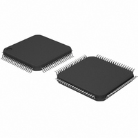
LPC1754FBD80,551 NXP Semiconductors, LPC1754FBD80,551 Datasheet - Page 2

LPC1754FBD80,551
Manufacturer Part Number
LPC1754FBD80,551
Description
IC ARM CORTEX MCU 128K 80-LQFP
Manufacturer
NXP Semiconductors
Series
LPC17xxr
Specifications of LPC1754FBD80,551
Program Memory Type
FLASH
Program Memory Size
128KB (128K x 8)
Package / Case
80-LQFP
Core Processor
ARM® Cortex-M3™
Core Size
32-Bit
Speed
100MHz
Connectivity
CAN, I²C, IrDA, Microwire, SPI, SSI, SSP, UART/USART, USB OTG
Peripherals
Brown-out Detect/Reset, DMA, Motor Control PWM, POR, PWM, WDT
Number Of I /o
52
Ram Size
32K x 8
Voltage - Supply (vcc/vdd)
2.4 V ~ 3.6 V
Data Converters
A/D 6x12b, D/A 1x10b
Oscillator Type
Internal
Operating Temperature
-40°C ~ 85°C
Processor Series
LPC17
Core
ARM Cortex M3
Data Bus Width
32 bit
Data Ram Size
32 KB
Interface Type
CAN, I2C, SPI, UART
Maximum Clock Frequency
100 MHz
Number Of Programmable I/os
52
Number Of Timers
3
Operating Supply Voltage
3.3 V
Maximum Operating Temperature
+ 85 C
Mounting Style
SMD/SMT
3rd Party Development Tools
MDK-ARM, RL-ARM, ULINK2
Minimum Operating Temperature
- 40 C
On-chip Adc
12 bit, 6 Channel
On-chip Dac
10 bit
Cpu Family
LPC17xx
Device Core
ARM Cortex-M3
Device Core Size
32b
Frequency (max)
100MHz
Total Internal Ram Size
32KB
# I/os (max)
52
Number Of Timers - General Purpose
4
Operating Supply Voltage (typ)
3.3V
Operating Supply Voltage (max)
3.6V
Operating Supply Voltage (min)
2.4/2.7V
Instruction Set Architecture
RISC
Operating Temp Range
-40C to 85C
Operating Temperature Classification
Industrial
Mounting
Surface Mount
Pin Count
80
Package Type
LQFP
Lead Free Status / RoHS Status
Lead free / RoHS Compliant
For Use With
622-1005 - USB IN-CIRCUIT PROG ARM7 LPC2K
Eeprom Size
-
Lead Free Status / Rohs Status
Lead free / RoHS Compliant
Other names
568-4790
935287913551
935287913551
Available stocks
Company
Part Number
Manufacturer
Quantity
Price
Company:
Part Number:
LPC1754FBD80,551
Manufacturer:
NXP Semiconductors
Quantity:
10 000
Part Number:
LPC1754FBD80,551
Manufacturer:
NXP/恩智浦
Quantity:
20 000
NXP Semiconductors
LPC1759_58_56_54_52_51
Product data sheet
Multilayer AHB matrix interconnect provides a separate bus for each AHB master.
AHB masters include the CPU, General Purpose DMA controller, Ethernet MAC
(LPC1758 only), and the USB interface. This interconnect provides communication
with no arbitration delays.
Split APB bus allows high throughput with few stalls between the CPU and DMA.
Serial interfaces:
Other peripherals:
On the LPC1758 only, Ethernet MAC with RMII interface and dedicated DMA
controller.
USB 2.0 full-speed device/Host/OTG controller with dedicated DMA controller and
on-chip PHY for device, Host, and OTG functions. The LPC1752/51 include a USB
device controller only.
Four UARTs with fractional baud rate generation, internal FIFO, and DMA support.
One UART has modem control I/O and RS-485/EIA-485 support, and one UART
has IrDA support.
CAN 2.0B controller with two (LPC1759/58/56) or one (LPC1754/52/51) channels.
SPI controller with synchronous, serial, full duplex communication and
programmable data length.
Two SSP controllers with FIFO and multi-protocol capabilities. The SSP interfaces
can be used with the GPDMA controller.
Two I
multiple address recognition and monitor mode.
On the LPC1759/58/56 only, I
output, with fractional rate control. The I
GPDMA. The I
receive as well as master clock input/output.
52 General Purpose I/O (GPIO) pins with configurable pull-up/down resistors. All
GPIOs support a new, configurable open-drain operating mode. The GPIO block is
accessed through the AHB multilayer bus for fast access and located in memory
such that it supports Cortex-M3 bit banding and use by the General Purpose DMA
Controller.
12-bit Analog-to-Digital Converter (ADC) with input multiplexing among six pins,
conversion rates up to 200 kHz, and multiple result registers. The 12-bit ADC can
be used with the GPDMA controller.
On the LPC1759/58/56/54 only, 10-bit Digital-to-Analog Converter (DAC) with
dedicated conversion timer and DMA support.
Four general purpose timers/counters, with a total of three capture inputs and ten
compare outputs. Each timer block has an external count input. Specific timer
events can be selected to generate DMA requests.
One motor control PWM with support for three-phase motor control.
Quadrature encoder interface that can monitor one external quadrature encoder.
One standard PWM/timer block with external count input.
Real-Time Clock (RTC) with a separate power domain and dedicated RTC
oscillator. The RTC block includes 20 bytes of battery-powered backup registers.
WatchDog Timer (WDT). The WDT can be clocked from the internal RC oscillator,
the RTC oscillator, or the APB clock.
ARM Cortex-M3 system tick timer, including an external clock input option.
2
C-bus interfaces supporting fast mode with a data rate of 400 kbit/s with
All information provided in this document is subject to legal disclaimers.
2
Rev. 6.01 — 11 March 2011
S-bus interface supports 3-wire and 4-wire data transmit and
2
S (Inter-IC Sound) interface for digital audio input or
LPC1759/58/56/54/52/51
2
S-bus interface can be used with the
32-bit ARM Cortex-M3 microcontroller
© NXP B.V. 2011. All rights reserved.
2 of 74


