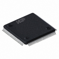
LPC1769FBD100,551 NXP Semiconductors, LPC1769FBD100,551 Datasheet - Page 35

LPC1769FBD100,551
Manufacturer Part Number
LPC1769FBD100,551
Description
IC ARM CORTEX MCU 512K 100-LQFP
Manufacturer
NXP Semiconductors
Series
LPC17xxr
Datasheets
1.OM11043.pdf
(79 pages)
2.LPC1767FBD100551.pdf
(2 pages)
3.LPC1767FBD100551.pdf
(840 pages)
4.LPC1769FBD100551.pdf
(66 pages)
Specifications of LPC1769FBD100,551
Program Memory Type
FLASH
Program Memory Size
512KB (512K x 8)
Package / Case
100-LQFP
Core Processor
ARM® Cortex-M3™
Core Size
32-Bit
Speed
120MHz
Connectivity
CAN, Ethernet, I²C, IrDA, Microwire, SPI, SSI, UART/USART, USB OTG
Peripherals
Brown-out Detect/Reset, DMA, I²S, Motor Control PWM, POR, PWM, WDT
Number Of I /o
70
Ram Size
64K x 8
Voltage - Supply (vcc/vdd)
2.4 V ~ 3.6 V
Data Converters
A/D 8x12b, D/A 1x10b
Oscillator Type
Internal
Operating Temperature
-40°C ~ 85°C
Processor Series
LPC17
Core
ARM Cortex M3
Data Bus Width
32 bit
Data Ram Size
64 KB
Interface Type
Ethernet, USB, OTG, CAN
Maximum Clock Frequency
120 MHz
Number Of Programmable I/os
70
Number Of Timers
4
Operating Supply Voltage
3.3 V
Maximum Operating Temperature
+ 85 C
Mounting Style
SMD/SMT
3rd Party Development Tools
MDK-ARM, RL-ARM, ULINK2, MCB1760, MCB1760U, MCB1760UME
Minimum Operating Temperature
- 40 C
On-chip Adc
12 bit, 8 Channel
On-chip Dac
10 bit
Lead Free Status / RoHS Status
Lead free / RoHS Compliant
For Use With
622-1005 - USB IN-CIRCUIT PROG ARM7 LPC2K
Eeprom Size
-
Lead Free Status / Rohs Status
Lead free / RoHS Compliant
Other names
568-4966
935290522551
935290522551
Available stocks
Company
Part Number
Manufacturer
Quantity
Price
Company:
Part Number:
LPC1769FBD100,551
Manufacturer:
NXP Semiconductors
Quantity:
10 000
NXP Semiconductors
LPC1769_68_67_66_65_64_63
Product data sheet
7.29.2 Main PLL (PLL0)
7.29.3 USB PLL (PLL1)
7.29.4 RTC clock output
7.29.5 Wake-up timer
The PLL0 accepts an input clock frequency in the range of 32 kHz to 25 MHz. The input
frequency is multiplied up to a high frequency, then divided down to provide the actual
clock used by the CPU and/or the USB block.
The PLL0 input, in the range of 32 kHz to 25 MHz, may initially be divided down by a
value ‘N’, which may be in the range of 1 to 256. This input division provides a wide range
of output frequencies from the same input frequency.
Following the PLL0 input divider is the PLL0 multiplier. This can multiply the input divider
output through the use of a Current Controlled Oscillator (CCO) by a value ‘M’, in the
range of 1 through 32768. The resulting frequency must be in the range of 275 MHz to
550 MHz. The multiplier works by dividing the CCO output by the value of M, then using a
phase-frequency detector to compare the divided CCO output to the multiplier input. The
error value is used to adjust the CCO frequency.
The PLL0 is turned off and bypassed following a chip Reset and by entering Power-down
mode. PLL0 is enabled by software only. The program must configure and activate the
PLL0, wait for the PLL0 to lock, and then connect to the PLL0 as a clock source.
The LPC17xx contain a second, dedicated USB PLL1 to provide clocking for the USB
interface.
The PLL1 receives its clock input from the main oscillator only and provides a fixed
48 MHz clock to the USB block only. The PLL1 is disabled and powered off on reset. If the
PLL1 is left disabled, the USB clock will be supplied by the 48 MHz clock from the main
PLL0.
The PLL1 accepts an input clock frequency in the range of 10 MHz to 25 MHz only. The
input frequency is multiplied up the range of 48 MHz for the USB clock using a Current
Controlled Oscillators (CCO). It is insured that the PLL1 output has a 50 % duty cycle.
The LPC17xx feature a clock output function intended for synchronizing with external
devices and for use during system development to allow checking the internal clocks
CCLK, IRC clock, main crystal, RTC clock, and USB clock in the outside world. The RTC
clock output allows tuning the RTC frequency without probing the pin, which would distort
the results.
The LPC17xx begin operation at power-up and when awakened from Power-down mode
by using the 4 MHz IRC oscillator as the clock source. This allows chip operation to
resume quickly. If the main oscillator or the PLL is needed by the application, software will
need to enable these features and wait for them to stabilize before they are used as a
clock source.
When the main oscillator is initially activated, the wake-up timer allows software to ensure
that the main oscillator is fully functional before the processor uses it as a clock source
and starts to execute instructions. This is important at power on, all types of Reset, and
All information provided in this document is subject to legal disclaimers.
Rev. 6.01 — 11 March 2011
LPC1769/68/67/66/65/64/63
32-bit ARM Cortex-M3 microcontroller
© NXP B.V. 2011. All rights reserved.
35 of 79


