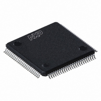
LPC1769FBD100,551 NXP Semiconductors, LPC1769FBD100,551 Datasheet - Page 55

LPC1769FBD100,551
Manufacturer Part Number
LPC1769FBD100,551
Description
IC ARM CORTEX MCU 512K 100-LQFP
Manufacturer
NXP Semiconductors
Series
LPC17xxr
Datasheets
1.OM11043.pdf
(79 pages)
2.LPC1767FBD100551.pdf
(2 pages)
3.LPC1767FBD100551.pdf
(840 pages)
4.LPC1769FBD100551.pdf
(66 pages)
Specifications of LPC1769FBD100,551
Program Memory Type
FLASH
Program Memory Size
512KB (512K x 8)
Package / Case
100-LQFP
Core Processor
ARM® Cortex-M3™
Core Size
32-Bit
Speed
120MHz
Connectivity
CAN, Ethernet, I²C, IrDA, Microwire, SPI, SSI, UART/USART, USB OTG
Peripherals
Brown-out Detect/Reset, DMA, I²S, Motor Control PWM, POR, PWM, WDT
Number Of I /o
70
Ram Size
64K x 8
Voltage - Supply (vcc/vdd)
2.4 V ~ 3.6 V
Data Converters
A/D 8x12b, D/A 1x10b
Oscillator Type
Internal
Operating Temperature
-40°C ~ 85°C
Processor Series
LPC17
Core
ARM Cortex M3
Data Bus Width
32 bit
Data Ram Size
64 KB
Interface Type
Ethernet, USB, OTG, CAN
Maximum Clock Frequency
120 MHz
Number Of Programmable I/os
70
Number Of Timers
4
Operating Supply Voltage
3.3 V
Maximum Operating Temperature
+ 85 C
Mounting Style
SMD/SMT
3rd Party Development Tools
MDK-ARM, RL-ARM, ULINK2, MCB1760, MCB1760U, MCB1760UME
Minimum Operating Temperature
- 40 C
On-chip Adc
12 bit, 8 Channel
On-chip Dac
10 bit
Lead Free Status / RoHS Status
Lead free / RoHS Compliant
For Use With
622-1005 - USB IN-CIRCUIT PROG ARM7 LPC2K
Eeprom Size
-
Lead Free Status / Rohs Status
Lead free / RoHS Compliant
Other names
568-4966
935290522551
935290522551
Available stocks
Company
Part Number
Manufacturer
Quantity
Price
Company:
Part Number:
LPC1769FBD100,551
Manufacturer:
NXP Semiconductors
Quantity:
10 000
NXP Semiconductors
LPC1769_68_67_66_65_64_63
Product data sheet
11.5 I
Table 13.
T
[1]
[2]
[3]
[4]
[5]
[6]
[7]
[8]
[9]
[10] A Fast-mode I
Symbol
f
t
t
t
t
t
2
SCL
f
LOW
HIGH
HD;DAT
SU;DAT
amb
C-bus
See the I
Parameters are valid over operating temperature range unless otherwise specified.
t
and the acknowledge.
A device must internally provide a hold time of at least 300 ns for the SDA signal (with respect to the
V
C
The maximum t
output stage t
SDA and the SCL pins and the SDA/SCL bus lines without exceeding the maximum specified t
In Fast-mode Plus, fall time is specified the same for both output stage and bus timing. If series resistors
are used, designers should allow for this when considering bus timing.
The maximum t
the maximum of t
maximum must only be met if the device does not stretch the LOW period (t
clock stretches the SCL, the data must be valid by the set-up time before it releases the clock.
t
transmission and the acknowledge.
250 ns must then be met. This will automatically be the case if the device does not stretch the LOW period
of the SCL signal. If such a device does stretch the LOW period of the SCL signal, it must output the next
data bit to the SDA line t
specification) before the SCL line is released. Also the acknowledge timing must meet this set-up time.
HD;DAT
SU;DAT
=
IH
b
−
= total capacitance of one bus line in pF.
(min) of the SCL signal) to bridge the undefined region of the falling edge of SCL.
40
is the data hold time that is measured from the falling edge of SCL; applies to data in transmission
is the data set-up time that is measured with respect to the rising edge of SCL; applies to data in
°
Dynamic characteristic: I
C to +85
2
C-bus specification UM10204 for details.
Parameter
SCL clock
frequency
fall time
LOW period of
the SCL clock
HIGH period of
the SCL clock
data hold time
data set-up
time
f
2
All information provided in this document is subject to legal disclaimers.
is specified at 250 ns. This allows series protection resistors to be connected in between the
C-bus device can be used in a Standard-mode I
HD;DAT
f
for the SDA and SCL bus lines is specified at 300 ns. The maximum fall time for the SDA
VD;DAT
°
C.
could be 3.45 μs and 0.9 μs for Standard-mode and Fast-mode but must be less than
Rev. 6.01 — 11 March 2011
[2]
or t
r(max)
VD;ACK
[4][5][6][7]
[3][4][8]
[9][10]
+ t
SU;DAT
by a transition time (see the I
LPC1769/68/67/66/65/64/63
2
= 1000 + 250 = 1250 ns (according to the Standard-mode I
C-bus pins
Conditions
Standard-mode
Fast-mode
Fast-mode Plus
of both SDA and
SCL signals
Standard-mode
Fast-mode
Fast-mode Plus
Standard-mode
Fast-mode
Fast-mode Plus
Standard-mode
Fast-mode
Fast-mode Plus
Standard-mode
Fast-mode
Fast-mode Plus
Standard-mode
Fast-mode
Fast-mode Plus
[1]
32-bit ARM Cortex-M3 microcontroller
2
C-bus system but the requirement t
2
C-bus specification UM10204). This
Min
0
0
0
-
20 + 0.1 × C
-
4.7
1.3
0.5
4.0
0.6
0.26
0
0
0
250
100
50
LOW
b
) of the SCL signal. If the
© NXP B.V. 2011. All rights reserved.
Max
100
400
1
300
300
120
-
-
-
-
-
-
-
-
-
-
-
-
f
.
Unit
kHz
kHz
MHz
ns
ns
ns
μs
μs
μs
μs
μs
μs
μs
μs
μs
ns
ns
ns
2
SU;DAT
55 of 79
C-bus
=


