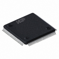
LPC2387FBD100,551 NXP Semiconductors, LPC2387FBD100,551 Datasheet - Page 5

LPC2387FBD100,551
Manufacturer Part Number
LPC2387FBD100,551
Description
IC ARM7 MCU FLASH 512K 100LQFP
Manufacturer
NXP Semiconductors
Series
LPC2300r
Specifications of LPC2387FBD100,551
Program Memory Type
FLASH
Program Memory Size
512KB (512K x 8)
Package / Case
100-LQFP
Core Processor
ARM7
Core Size
16/32-Bit
Speed
72MHz
Connectivity
CAN, Ethernet, I²C, Microwire, MMC, SPI, SSI, SSP, UART/USART, USB OTG
Peripherals
Brown-out Detect/Reset, DMA, I²S, POR, PWM, WDT
Number Of I /o
70
Ram Size
98K x 8
Voltage - Supply (vcc/vdd)
3 V ~ 3.6 V
Data Converters
A/D 6x10b; D/A 1x10b
Oscillator Type
Internal
Operating Temperature
-40°C ~ 85°C
Processor Series
LPC23
Core
ARM7TDMI-S
Data Bus Width
16 bit, 32 bit
Data Ram Size
98 KB
Interface Type
CAN/I2C/I2S/SSP/UART/USB
Maximum Clock Frequency
72 MHz
Number Of Programmable I/os
70
Number Of Timers
4
Operating Supply Voltage
3.3 V
Maximum Operating Temperature
+ 85 C
Mounting Style
SMD/SMT
3rd Party Development Tools
MDK-ARM, RL-ARM, ULINK2, MCB2387, MCB2387U, MCB2387UME
Development Tools By Supplier
OM11013
Minimum Operating Temperature
- 40 C
On-chip Adc
6-ch x 10-bit
On-chip Dac
1-ch x 10-bit
Cpu Family
LPC2000
Device Core
ARM7TDMI-S
Device Core Size
16/32Bit
Frequency (max)
72MHz
Total Internal Ram Size
98KB
# I/os (max)
70
Number Of Timers - General Purpose
4
Operating Supply Voltage (typ)
3.3V
Operating Supply Voltage (max)
3.6V
Operating Supply Voltage (min)
3V
Instruction Set Architecture
RISC
Operating Temp Range
-40C to 85C
Operating Temperature Classification
Industrial
Mounting
Surface Mount
Pin Count
100
Package Type
LQFP
Lead Free Status / RoHS Status
Lead free / RoHS Compliant
For Use With
568-4359 - BOARD EVAL FOR LPC2387568-4310 - EVAL BOARD LPC2158 W/LCD568-3999 - BOARD EVAL FOR LPC23 ARM MCU622-1005 - USB IN-CIRCUIT PROG ARM7 LPC2K
Eeprom Size
-
Lead Free Status / Rohs Status
Compliant
Other names
568-4322
935284932551
LPC2387FBD100-S
935284932551
LPC2387FBD100-S
Available stocks
Company
Part Number
Manufacturer
Quantity
Price
Company:
Part Number:
LPC2387FBD100,551
Manufacturer:
NXP Semiconductors
Quantity:
10 000
NXP Semiconductors
6. Pinning information
Table 3.
LPC2387
Product data sheet
Symbol
P0[0] to P0[31]
P0[0]/RD1/TXD3/
SDA1
P0[1]/TD1/RXD3/
SCL1
P0[2]/TXD0
P0[3]/RXD0
P0[4]/I2SRX_CLK/
RD2/CAP2[0]
Fig 2.
LPC2387 pinning LQFP100 package
Pin description
6.1 Pinning
6.2 Pin description
Pin
46
47
98
99
81
[1]
[1]
[1]
[1]
[1]
Type
I/O
I/O
I
O
I/O
I/O
O
I
I/O
I/O
O
I/O
I
I/O
I/O
I
I
All information provided in this document is subject to legal disclaimers.
Description
Port 0: Port 0 is a 32-bit I/O port with individual direction controls for each bit.
The operation of port 0 pins depends upon the pin function selected via the pin
connect block. Pins 12, 13, 14, and 31 of this port are not available.
P0[0] — General purpose digital input/output pin.
RD1 — CAN1 receiver input.
TXD3 — Transmitter output for UART3.
SDA1 — I
P0[1] — General purpose digital input/output pin.
TD1 — CAN1 transmitter output.
RXD3 — Receiver input for UART3.
SCL1 — I
P0[2] — General purpose digital input/output pin.
TXD0 — Transmitter output for UART0.
P0[3] — General purpose digital input/output pin.
RXD0 — Receiver input for UART0.
P0[4] — General purpose digital input/output pin.
I2SRX_CLK — Receive Clock. It is driven by the master and received by the
slave. Corresponds to the signal SCK in the I
RD2 — CAN2 receiver input.
CAP2[0] — Capture input for Timer 2, channel 0.
25
1
Rev. 4 — 10 February 2011
LPC2387FBD100
2
2
C1 clock input/output (this is not an open-drain pin).
C1 data input/output (this is not an open-drain pin).
002aad329
75
51
2
S-bus specification.
Single-chip 16-bit/32-bit MCU
LPC2387
© NXP B.V. 2011. All rights reserved.
5 of 64


