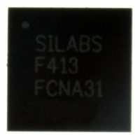
C8051F413-GM Silicon Laboratories Inc, C8051F413-GM Datasheet - Page 29

C8051F413-GM
Manufacturer Part Number
C8051F413-GM
Description
IC 8051 MCU 16K FLASH 28QFN
Manufacturer
Silicon Laboratories Inc
Series
C8051F41xr
Specifications of C8051F413-GM
Program Memory Type
FLASH
Program Memory Size
16KB (16K x 8)
Package / Case
28-QFN
Core Processor
8051
Core Size
8-Bit
Speed
50MHz
Connectivity
SMBus (2-Wire/I²C), SPI, UART/USART
Peripherals
Brown-out Detect/Reset, POR, PWM, Temp Sensor, WDT
Number Of I /o
20
Ram Size
2.25K x 8
Voltage - Supply (vcc/vdd)
2 V ~ 5.25 V
Data Converters
A/D 20x12b; D/A 2x12b
Oscillator Type
Internal
Operating Temperature
-40°C ~ 85°C
Processor Series
C8051F4x
Core
8051
Data Bus Width
8 bit
Data Ram Size
2.25 KB
Interface Type
I2C/SMBus/SPI/UART
Maximum Clock Frequency
50 MHz
Number Of Programmable I/os
20
Number Of Timers
4
Operating Supply Voltage
2 V to 5.25 V
Maximum Operating Temperature
+ 85 C
Mounting Style
SMD/SMT
3rd Party Development Tools
PK51, CA51, A51, ULINK2
Development Tools By Supplier
C8051F410DK
Minimum Operating Temperature
- 40 C
On-chip Dac
2-ch x 12-bit
Lead Free Status / RoHS Status
Lead free / RoHS Compliant
For Use With
770-1006 - ISP 4PORT FOR SILABS C8051F MCU336-1454 - ADAPTER PROGRAM TOOLSTICK F411336-1317 - KIT EVAL FOR C8051F411336-1314 - KIT DEV FOR C8051F41X
Eeprom Size
-
Lead Free Status / Rohs Status
Lead free / RoHS Compliant
Other names
336-1311
Available stocks
Company
Part Number
Manufacturer
Quantity
Price
Company:
Part Number:
C8051F413-GM
Manufacturer:
Silicon Labs
Quantity:
135
Part Number:
C8051F413-GM
Manufacturer:
SILICON LABS/芯科
Quantity:
20 000
Company:
Part Number:
C8051F413-GMR
Manufacturer:
M/A-COM
Quantity:
1 001
Part Number:
C8051F413-GMR
Manufacturer:
SILICON LABS/芯科
Quantity:
20 000
1.5.
The C8051F41x devices include an on-chip 12-bit SAR ADC with a 27-channel single-ended input multi-
plexer and a maximum throughput of 200 ksps. The ADC system includes a configurable analog multi-
plexer that selects the positive ADC input, which is measured with respect to GND. Ports 0–2 are available
as ADC inputs; additionally, the on-chip Temperature Sensor output and the core supply voltage (V
available as ADC inputs. User firmware may shut down the ADC or use it in Burst Mode to save power.
Conversions can be started in four ways: a software command, an overflow of Timer 2 or 3, or an external
convert start signal. This flexibility allows the start of conversion to be triggered by software events, a peri-
odic signal (timer overflows), or external HW signals. Conversion completions are indicated by a status bit
and an interrupt (if enabled) and occur after 1, 4, 8, or 16 samples have been accumulated by a hardware
accumulator. The resulting data word is latched into the ADC data SFRs upon completion of a conversion.
When the system clock is slow, Burst Mode allows ADC0 to automatically wake from a low power shut-
down state, acquire and accumulate samples, then re-enter the low power shutdown state without CPU
intervention.
Window compare registers for the ADC data can be configured to interrupt the controller when ADC data is
either within or outside of a specified range. The ADC can monitor a key voltage continuously in back-
ground mode, but not interrupt the controller unless the converted data is within/outside the specified
range.
1.6.
The C8051F41x devices include two 12-bit current-mode Digital-to-Analog Converters (IDACs). The maxi-
mum current output of the IDACs can be adjusted for four different current settings; 0.25 mA, 0.5 mA,
1 mA, and 2 mA. A flexible output update mechanism allows for seamless full-scale changes, and supports
jitter-free updates for waveform generation. The IDAC outputs can be merged onto a single port I/O pin for
increased full-scale current output or increased resolution. IDAC updates can be performed on-demand,
scheduled on a Timer overflow, or synchronized with an external signal. Figure 1.8 shows a block diagram
of the IDAC circuitry.
C8051F410/2
available on
P2.3-2.6
12-Bit Analog to Digital Converter
Two 12-bit Current-Mode DACs
Sensor
Temp
Analog Multiplexer
GND
VDD
P0.0
P0.7
P1.0
P1.7
P2.0
P2.7
Figure 1.7. 12-Bit ADC Block Diagram
19-to-1
AMUX
Configuration, Control, and Data Registers
Burst Mode
Logic
Rev. 1.1
ADC
12-Bit
SAR
End of
Conversion
Interrupt
C8051F410/1/2/3
Conversion
Start
Window Compare
16
Logic
Accumulator
AD0BUSY (W)
Timer 3 Overflow
CNVSTR Rising Edge
Timer 2 Overflow
ADC Data
Registers
Window
Compare
Interrupt
DD
) are
29


