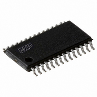
P89LPC931FDH,112 NXP Semiconductors, P89LPC931FDH,112 Datasheet - Page 32

P89LPC931FDH,112
Manufacturer Part Number
P89LPC931FDH,112
Description
IC 80C51 MCU FLASH 8K 28-TSSOP
Manufacturer
NXP Semiconductors
Series
LPC900r
Datasheet
1.P89LPC931FDH112.pdf
(55 pages)
Specifications of P89LPC931FDH,112
Core Processor
8051
Core Size
8-Bit
Speed
12MHz
Connectivity
I²C, SPI, UART/USART
Peripherals
Brown-out Detect/Reset, LED, POR, PWM, WDT
Number Of I /o
26
Program Memory Size
8KB (8K x 8)
Program Memory Type
FLASH
Ram Size
256 x 8
Voltage - Supply (vcc/vdd)
2.4 V ~ 3.6 V
Oscillator Type
Internal
Operating Temperature
-40°C ~ 85°C
Package / Case
28-TSSOP
Processor Series
P89LPC9x
Core
80C51
Data Bus Width
8 bit
Data Ram Size
256 B
Interface Type
I2C, SPI, UART
Maximum Clock Frequency
18 MHz
Number Of Programmable I/os
26
Number Of Timers
2
Operating Supply Voltage
2.4 V to 3.6 V
Maximum Operating Temperature
+ 85 C
Mounting Style
SMD/SMT
3rd Party Development Tools
PK51, CA51, A51, ULINK2
Minimum Operating Temperature
- 45 C
For Use With
622-1014 - BOARD FOR LPC9XX TSSOP622-1008 - BOARD FOR LPC9103 10-HVSON622-1006 - SOCKET ADAPTER BOARDMCB900K - BOARD PROTOTYPE NXP 89LPC9EPM900K - EMULATOR/PROGRAMMER NXP P89LPC9568-4000 - DEMO BOARD SPI/I2C TO DUAL UART568-3510 - DEMO BOARD SPI/I2C TO UART622-1002 - USB IN-CIRCUIT PROG LPC9XX568-1759 - EMULATOR DEBUGGER/PROGRMMR LPC9X568-1758 - BOARD EVAL FOR LPC93X MCU FAMILY
Lead Free Status / RoHS Status
Lead free / RoHS Compliant
Eeprom Size
-
Data Converters
-
Lead Free Status / Rohs Status
Details
Other names
568-1284-5
935273877112
P89LPC931FDH
P89LPC931FDH,129
P89LPC931FDH-S
935273877112
P89LPC931FDH
P89LPC931FDH,129
P89LPC931FDH-S
Philips Semiconductors
9397 750 14472
Product data
Fig 9. SPI block diagram.
SPI STATUS REGISTER
BY 4, 16, 64, 128
CPU clock
DIVIDER
SELECT
SPI CONTROL
The SPI interface has four pins: SPICLK, MOSI, MISO, and SS:
Typical connections are shown in Figures 10, 11, and 12.
•
•
interrupt
request
SPI clock (master)
SPICLK, MOSI and MISO are typically tied together between two or more SPI
devices. Data flows from master to slave on MOSI (Master Out Slave In) pin and
flows from slave to master on MISO (Master In Slave Out) pin. The SPICLK signal
is output in the master mode and is input in the slave mode. If the SPI system is
disabled, i.e. SPEN (SPCTL.6) = 0 (reset value), these pins are configured for port
functions.
SS is the optional slave select pin. In a typical configuration, an SPI master asserts
one of its port pins to select one SPI device as the current slave. An SPI slave
device uses its SS pin to determine whether it is selected.
SPI
MSTR
SPEN
Rev. 05 — 15 December 2004
internal
data
bus
SPI CONTROL REGISTER
8-BIT SHIFT REGISTER
READ DATA BUFFER
CLOCK LOGIC
8-bit microcontrollers with two-clock 80C51 core
clock
P89LPC930/931
© Koninklijke Philips Electronics N.V. 2004. All rights reserved.
M
M
M
S
S
S
002aaa434
SPICLK
MISO
MOSI
P2.3
P2.2
P2.5
P2.4
SS
32 of 55


