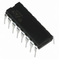
ST7FLITE09Y0B6 STMicroelectronics, ST7FLITE09Y0B6 Datasheet - Page 27

ST7FLITE09Y0B6
Manufacturer Part Number
ST7FLITE09Y0B6
Description
MCU 8BIT 1.5KB FLASH 128KB 16DIP
Manufacturer
STMicroelectronics
Series
ST7r
Datasheet
1.ST7FLITES2Y0B6.pdf
(124 pages)
Specifications of ST7FLITE09Y0B6
Core Processor
ST7
Core Size
8-Bit
Speed
8MHz
Connectivity
SPI
Peripherals
Brown-out Detect/Reset, POR, PWM, WDT
Number Of I /o
13
Program Memory Size
1.5KB (1.5K x 8)
Program Memory Type
FLASH
Eeprom Size
128 x 8
Ram Size
128 x 8
Voltage - Supply (vcc/vdd)
2.4 V ~ 5.5 V
Data Converters
A/D 5x8b
Oscillator Type
Internal
Operating Temperature
-40°C ~ 85°C
Package / Case
16-DIP (0.300", 7.62mm)
Processor Series
ST7FLITE0x
Core
ST7
Data Bus Width
8 bit
Data Ram Size
128 B
Interface Type
SPI
Maximum Clock Frequency
8 MHz
Number Of Programmable I/os
13
Number Of Timers
2
Operating Supply Voltage
2.4 V to 5.5 V
Maximum Operating Temperature
+ 85 C
Mounting Style
Through Hole
Development Tools By Supplier
ST7FLIT0-IND/USB, ST7FLIT2-COS/COM, ST7FLITE-SK/RAIS, ST7MDT10-DVP3, ST7MDT10-EMU3, STX-RLINK
Minimum Operating Temperature
- 40 C
On-chip Adc
8 bit
For Use With
497-6250 - BOARD RGB COLOR CTRL STP04CM596497-5858 - EVAL BOARD PLAYBACK ST7FLITE497-5049 - KIT STARTER RAISONANCE ST7FLITE497-5046 - KIT TOOL FOR ST7/UPSD/STR7 MCU
Lead Free Status / RoHS Status
Lead free / RoHS Compliant
Other names
497-5632-5
Available stocks
Company
Part Number
Manufacturer
Quantity
Price
Company:
Part Number:
ST7FLITE09Y0B6
Manufacturer:
Maestro
Quantity:
1 200
Company:
Part Number:
ST7FLITE09Y0B6
Manufacturer:
STMicroelectronics
Quantity:
135
7.4 RESET SEQUENCE MANAGER (RSM)
7.4.1 Introduction
The reset sequence manager includes three RE-
SET sources as shown in
■
■
■
Note: A reset can also be triggered following the
detection of an illegal opcode or prebyte code. Re-
fer to
These sources act on the RESET pin and it is al-
ways kept low during the delay phase.
The RESET service routine vector is fixed at ad-
dresses FFFEh-FFFFh in the ST7 memory map.
The basic RESET sequence consists of 3 phases
as shown in
■
■
■
Figure 16.Reset Block Diagram
External RESET source pulse
Internal LVD RESET (Low Voltage Detection)
Internal WATCHDOG RESET
Active Phase depending on the RESET source
256 CPU clock cycle delay
RESET vector fetch
Note 1: See “Illegal Opcode Reset” on page 78. for more details on illegal opcode reset conditions.
RESET
section 11.2.1 on page 53
Figure
15:
V
Figure
DD
R
ON
for further details.
16:
FILTER
GENERATOR
PULSE
The 256 CPU clock cycle delay allows the oscilla-
tor to stabilise and ensures that recovery has tak-
en place from the Reset state.
The RESET vector fetch phase duration is 2 clock
cycles.
If the PLL is enabled by option byte, it outputs the
clock after an additional delay of t
Figure
Figure 15. RESET Sequence Phases
Active Phase
13).
ST7LITE0xY0, ST7LITESxY0
WATCHDOG RESET
ILLEGAL OPCODE RESET
LVD RESET
256 CLOCK CYCLES
INTERNAL RESET
RESET
INTERNAL
RESET
STARTUP
VECTOR
FETCH
1)
27/124
(see
1


