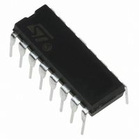
ST7FLITE09Y0B6 STMicroelectronics, ST7FLITE09Y0B6 Datasheet - Page 42

ST7FLITE09Y0B6
Manufacturer Part Number
ST7FLITE09Y0B6
Description
MCU 8BIT 1.5KB FLASH 128KB 16DIP
Manufacturer
STMicroelectronics
Series
ST7r
Datasheet
1.ST7FLITES2Y0B6.pdf
(124 pages)
Specifications of ST7FLITE09Y0B6
Core Processor
ST7
Core Size
8-Bit
Speed
8MHz
Connectivity
SPI
Peripherals
Brown-out Detect/Reset, POR, PWM, WDT
Number Of I /o
13
Program Memory Size
1.5KB (1.5K x 8)
Program Memory Type
FLASH
Eeprom Size
128 x 8
Ram Size
128 x 8
Voltage - Supply (vcc/vdd)
2.4 V ~ 5.5 V
Data Converters
A/D 5x8b
Oscillator Type
Internal
Operating Temperature
-40°C ~ 85°C
Package / Case
16-DIP (0.300", 7.62mm)
Processor Series
ST7FLITE0x
Core
ST7
Data Bus Width
8 bit
Data Ram Size
128 B
Interface Type
SPI
Maximum Clock Frequency
8 MHz
Number Of Programmable I/os
13
Number Of Timers
2
Operating Supply Voltage
2.4 V to 5.5 V
Maximum Operating Temperature
+ 85 C
Mounting Style
Through Hole
Development Tools By Supplier
ST7FLIT0-IND/USB, ST7FLIT2-COS/COM, ST7FLITE-SK/RAIS, ST7MDT10-DVP3, ST7MDT10-EMU3, STX-RLINK
Minimum Operating Temperature
- 40 C
On-chip Adc
8 bit
For Use With
497-6250 - BOARD RGB COLOR CTRL STP04CM596497-5858 - EVAL BOARD PLAYBACK ST7FLITE497-5049 - KIT STARTER RAISONANCE ST7FLITE497-5046 - KIT TOOL FOR ST7/UPSD/STR7 MCU
Lead Free Status / RoHS Status
Lead free / RoHS Compliant
Other names
497-5632-5
Available stocks
Company
Part Number
Manufacturer
Quantity
Price
Company:
Part Number:
ST7FLITE09Y0B6
Manufacturer:
Maestro
Quantity:
1 200
Company:
Part Number:
ST7FLITE09Y0B6
Manufacturer:
STMicroelectronics
Quantity:
135
ST7LITE0xY0, ST7LITESxY0
10 I/O PORTS
10.1 INTRODUCTION
The I/O ports offer different functional modes:
– transfer of data through digital inputs and outputs
and for specific pins:
– external interrupt generation
– alternate signal input/output for the on-chip pe-
An I/O port contains up to 8 pins. Each pin can be
programmed independently as digital input (with or
without interrupt generation) or digital output.
10.2 FUNCTIONAL DESCRIPTION
Each port has 2 main registers:
– Data Register (DR)
– Data Direction Register (DDR)
and one optional register:
– Option Register (OR)
Each I/O pin may be programmed using the corre-
sponding register bits in the DDR and OR regis-
ters: bit X corresponding to pin X of the port. The
same correspondence is used for the DR register.
The following description takes into account the
OR register, (for specific ports which do not pro-
vide this register refer to the I/O Port Implementa-
tion section). The generic I/O block diagram is
shown in
10.2.1 Input Modes
The input configuration is selected by clearing the
corresponding DDR register bit.
In this case, reading the DR register returns the
digital value applied to the external I/O pin.
Different input modes can be selected by software
through the OR register.
Note: Writing the DR register modifies the latch
value but does not affect the pin status.
External interrupt function
When an I/O is configured as Input with Interrupt,
an event on this I/O can generate an external inter-
rupt request to the CPU.
Each pin can independently generate an interrupt
request. The interrupt sensitivity is independently
programmable using the sensitivity bits in the
EICR register.
Each external interrupt vector is linked to a dedi-
cated group of I/O port pins (see pinout description
and interrupt section). If several input pins are se-
lected simultaneously as interrupt source, these
42/124
1
ripherals.
Figure 29
are logically ANDed. For this reason if one of the
interrupt pins is tied low, it may mask the others.
External interrupts are hardware interrupts. Fetch-
ing the corresponding interrupt vector automatical-
ly clears the request latch. Changing the sensitivity
of a particular external interrupt clears this pending
interrupt. This can be used to clear unwanted
pending interrupts.
Spurious interrupts
When enabling/disabling an external interrupt by
setting/resetting the related OR register bit, a spu-
rious interrupt is generated if the pin level is low
and its edge sensitivity includes falling/rising edge.
This is due to the edge detector input which is
switched to '1' when the external interrupt is disa-
bled by the OR register.
To avoid this unwanted interrupt, a "safe" edge
sensitivity (rising edge for enabling and falling
edge for disabling) has to be selected before
changing the OR register bit and configuring the
appropriate sensitivity again.
Caution: In case a pin level change occurs during
these operations (asynchronous signal input), as
interrupts are generated according to the current
sensitivity, it is advised to disable all interrupts be-
fore and to reenable them after the complete pre-
vious sequence in order to avoid an external inter-
rupt occurring on the unwanted edge.
This corresponds to the following steps:
1. To enable an external interrupt:
2. To disable an external interrupt:
– set the interrupt mask with the SIM instruction
– select rising edge
– enable the external interrupt through the OR
– select the desired sensitivity if different from
– reset the interrupt mask with the RIM instruc-
– set the interrupt mask with the SIM instruction
– select falling edge
– disable the external interrupt through the OR
– select rising edge
(in cases where a pin level change could oc-
cur)
register
rising edge
tion (in cases where a pin level change could
occur)
SIM (in cases where a pin level change could
occur)
register


