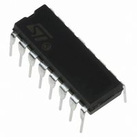
ST7FLITE09Y0B6 STMicroelectronics, ST7FLITE09Y0B6 Datasheet - Page 68

ST7FLITE09Y0B6
Manufacturer Part Number
ST7FLITE09Y0B6
Description
MCU 8BIT 1.5KB FLASH 128KB 16DIP
Manufacturer
STMicroelectronics
Series
ST7r
Datasheet
1.ST7FLITES2Y0B6.pdf
(124 pages)
Specifications of ST7FLITE09Y0B6
Core Processor
ST7
Core Size
8-Bit
Speed
8MHz
Connectivity
SPI
Peripherals
Brown-out Detect/Reset, POR, PWM, WDT
Number Of I /o
13
Program Memory Size
1.5KB (1.5K x 8)
Program Memory Type
FLASH
Eeprom Size
128 x 8
Ram Size
128 x 8
Voltage - Supply (vcc/vdd)
2.4 V ~ 5.5 V
Data Converters
A/D 5x8b
Oscillator Type
Internal
Operating Temperature
-40°C ~ 85°C
Package / Case
16-DIP (0.300", 7.62mm)
Processor Series
ST7FLITE0x
Core
ST7
Data Bus Width
8 bit
Data Ram Size
128 B
Interface Type
SPI
Maximum Clock Frequency
8 MHz
Number Of Programmable I/os
13
Number Of Timers
2
Operating Supply Voltage
2.4 V to 5.5 V
Maximum Operating Temperature
+ 85 C
Mounting Style
Through Hole
Development Tools By Supplier
ST7FLIT0-IND/USB, ST7FLIT2-COS/COM, ST7FLITE-SK/RAIS, ST7MDT10-DVP3, ST7MDT10-EMU3, STX-RLINK
Minimum Operating Temperature
- 40 C
On-chip Adc
8 bit
For Use With
497-6250 - BOARD RGB COLOR CTRL STP04CM596497-5858 - EVAL BOARD PLAYBACK ST7FLITE497-5049 - KIT STARTER RAISONANCE ST7FLITE497-5046 - KIT TOOL FOR ST7/UPSD/STR7 MCU
Lead Free Status / RoHS Status
Lead free / RoHS Compliant
Other names
497-5632-5
Available stocks
Company
Part Number
Manufacturer
Quantity
Price
Company:
Part Number:
ST7FLITE09Y0B6
Manufacturer:
Maestro
Quantity:
1 200
Company:
Part Number:
ST7FLITE09Y0B6
Manufacturer:
STMicroelectronics
Quantity:
135
ST7LITE0xY0, ST7LITESxY0
SERIAL PERIPHERAL INTERFACE (Cont’d)
CONTROL/STATUS REGISTER (SPICSR)
Read/Write (some bits Read Only)
Reset Value: 0000 0000 (00h)
Bit 7 = SPIF Serial Peripheral Data Transfer Flag
0: Data transfer is in progress or the flag has been
1: Data transfer between the device and an exter-
Note: While the SPIF bit is set, all writes to the
SPIDR register are inhibited until the SPICSR reg-
ister is read.
Bit 6 = WCOL Write Collision status (Read only).
This bit is set by hardware when a write to the
SPIDR register is done during a transmit se-
quence. It is cleared by a software sequence (see
Figure
0: No write collision occurred
1: A write collision has been detected
Bit 5 = OVR SPI Overrun error (Read only).
This bit is set by hardware when the byte currently
being received in the shift register is ready to be
transferred into the SPIDR register while SPIF = 1
(See
SPIE = 1 in the SPICR register. The OVR bit is
cleared by software reading the SPICSR register.
0: No overrun error
1: Overrun error detected
Bit 4 = MODF Mode Fault flag (Read only).
This bit is set by hardware when the SS pin is
pulled low in master mode (see
Master Mode Fault
be generated if SPIE=1 in the SPICR register. This
bit is cleared by a software sequence (An access
to the SPICSR register while MODF=1 followed by
a write to the SPICR register).
0: No master mode fault detected
1: A fault in master mode has been detected
68/124
1
SPIF
cleared.
nal device has been completed.
(Read only).
This bit is set by hardware when a transfer has
been completed. An interrupt is generated if
SPIE=1 in the SPICR register. It is cleared by a
software sequence (an access to the SPICSR
register followed by a write or a read to the
SPIDR register).
7
Section
42).
WCOL
11.3.5.2). An interrupt is generated if
OVR
(MODF)). An SPI interrupt can
MODF
-
Section 11.3.5.1
SOD
SSM
SSI
0
Bit 3 = Reserved, must be kept cleared.
Bit 2 = SOD SPI Output Disable.
This bit is set and cleared by software. When set, it
disables the alternate function of the SPI output
(MOSI in master mode / MISO in slave mode)
0: SPI output enabled (if SPE=1)
1: SPI output disabled
Bit 1 = SSM SS Management.
This bit is set and cleared by software. When set, it
disables the alternate function of the SPI SS pin
and uses the SSI bit value instead. See
11.3.3.2 Slave Select
0: Hardware management (SS managed by exter-
1: Software management (internal SS signal con-
Bit 0 = SSI SS Internal Mode.
This bit is set and cleared by software. It acts as a
‘chip select’ by controlling the level of the SS slave
select signal when the SSM bit is set.
0 : Slave selected
1 : Slave deselected
DATA I/O REGISTER (SPIDR)
Read/Write
Reset Value: Undefined
The SPIDR register is used to transmit and receive
data on the serial bus. In a master device, a write
to this register will initiate transmission/reception
of another byte.
Notes: During the last clock cycle the SPIF bit is
set, a copy of the received data byte in the shift
register is moved to a buffer. When the user reads
the serial peripheral data I/O register, the buffer is
actually being read.
While the SPIF bit is set, all writes to the SPIDR
register are inhibited until the SPICSR register is
read.
Warning: A write to the SPIDR register places
data directly into the shift register for transmission.
A read to the SPIDR register returns the value lo-
cated in the buffer and not the content of the shift
register (see
D7
nal pin)
trolled by SSI bit. External SS pin free for gener-
al-purpose I/O)
7
D6
Figure
D5
37).
D4
Management.
D3
D2
D1
Section
D0
0


