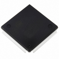
ST10F272Z2Q3 STMicroelectronics, ST10F272Z2Q3 Datasheet - Page 100

ST10F272Z2Q3
Manufacturer Part Number
ST10F272Z2Q3
Description
MCU 16BIT 256KB FLASH 144-PQFP
Manufacturer
STMicroelectronics
Series
ST10r
Datasheet
1.ST10F272Z2Q3.pdf
(189 pages)
Specifications of ST10F272Z2Q3
Core Processor
ST10
Core Size
16-Bit
Speed
64MHz
Connectivity
ASC, CAN, EBI/EMI, I²C, SSC, UART/USART
Peripherals
POR, PWM, WDT
Number Of I /o
111
Program Memory Size
256KB (256K x 8)
Program Memory Type
FLASH
Ram Size
20K x 8
Voltage - Supply (vcc/vdd)
4.5 V ~ 5.5 V
Data Converters
A/D 24x10b
Oscillator Type
Internal
Operating Temperature
-40°C ~ 125°C
Package / Case
144-QFP
Lead Free Status / RoHS Status
Lead free / RoHS Compliant
Eeprom Size
-
Other names
497-5579
Available stocks
Company
Part Number
Manufacturer
Quantity
Price
Company:
Part Number:
ST10F272Z2Q3
Manufacturer:
E-CMOS
Quantity:
10 000
Company:
Part Number:
ST10F272Z2Q3
Manufacturer:
STMicroelectronics
Quantity:
10 000
- Current page: 100 of 189
- Download datasheet (4Mb)
System reset
100/189
To ensure correct power-up reset with controlled supply current consumption, specially if
clock signal requires a long period of time to stabilize, an asynchronous hardware reset is
required during power-up. For this reason, it is recommended to connect the external R0-C0
circuit shown in Figure 30 to the RPD pin. On power-up, the logical low level on RPD pin
forces an asynchronous hardware reset when RSTIN is asserted low. The external pull-up
R0 will then charge the capacitor C0. Note that an internal pull-down device on RPD pin is
turned on when RSTIN pin is low, and causes the external capacitor (C0) to begin
discharging at a typical rate of 100-200 µA. With this mechanism, after power-up reset,
short low pulses applied on RSTIN produce synchronous hardware reset. If RSTIN is
asserted longer than the time needed for C0 to be discharged by the internal pull-down
device, then the device is forced in an asynchronous reset. This mechanism insures
recovery from very catastrophic failure.
Figure 30. Minimum external reset circuitry
The minimum reset circuit of
the ST10F272Z2 itself during software or watchdog triggered resets, because of the
capacitor C1 that will keep the voltage on RSTIN pin above V
reset sequence, and thus will trigger an asynchronous reset sequence.
Figure 31 shows an example of a reset circuit. In this example, R1-C1 external circuit is only
used to generate power-up or manual reset, and R0-C0 circuit on RPD is used for power-up
reset and to exit from Power Down mode. Diode D1 creates a wired-OR gate connection to
the reset pin and may be replaced by open-collector Schmitt trigger buffer. Diode D2
provides a faster cycle time for repetitive power-on resets.
R2 is an optional pull-up for faster recovery and correct biasing of TTL Open Collector
drivers.
ST10F272
Figure 30
RSTOUT
RSTIN
RPD
is not adequate when the RSTIN pin is driven from
+
+
V
CC
R0
C0
C1
External Hardware
(and Interruptible
Power Down
mode)
b) For Power-up
Reset
a) Hardware
Reset
IL
after the end of the internal
ST10F272Z2
Related parts for ST10F272Z2Q3
Image
Part Number
Description
Manufacturer
Datasheet
Request
R

Part Number:
Description:
STMicroelectronics [RIPPLE-CARRY BINARY COUNTER/DIVIDERS]
Manufacturer:
STMicroelectronics
Datasheet:

Part Number:
Description:
STMicroelectronics [LIQUID-CRYSTAL DISPLAY DRIVERS]
Manufacturer:
STMicroelectronics
Datasheet:

Part Number:
Description:
BOARD EVAL FOR MEMS SENSORS
Manufacturer:
STMicroelectronics
Datasheet:

Part Number:
Description:
NPN TRANSISTOR POWER MODULE
Manufacturer:
STMicroelectronics
Datasheet:

Part Number:
Description:
TURBOSWITCH ULTRA-FAST HIGH VOLTAGE DIODE
Manufacturer:
STMicroelectronics
Datasheet:

Part Number:
Description:
Manufacturer:
STMicroelectronics
Datasheet:

Part Number:
Description:
DIODE / SCR MODULE
Manufacturer:
STMicroelectronics
Datasheet:

Part Number:
Description:
DIODE / SCR MODULE
Manufacturer:
STMicroelectronics
Datasheet:

Part Number:
Description:
Search -----> STE16N100
Manufacturer:
STMicroelectronics
Datasheet:

Part Number:
Description:
Search ---> STE53NA50
Manufacturer:
STMicroelectronics
Datasheet:

Part Number:
Description:
NPN Transistor Power Module
Manufacturer:
STMicroelectronics
Datasheet:


