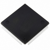
ST10F272Z2Q3 STMicroelectronics, ST10F272Z2Q3 Datasheet - Page 151

ST10F272Z2Q3
Manufacturer Part Number
ST10F272Z2Q3
Description
MCU 16BIT 256KB FLASH 144-PQFP
Manufacturer
STMicroelectronics
Series
ST10r
Datasheet
1.ST10F272Z2Q3.pdf
(189 pages)
Specifications of ST10F272Z2Q3
Core Processor
ST10
Core Size
16-Bit
Speed
64MHz
Connectivity
ASC, CAN, EBI/EMI, I²C, SSC, UART/USART
Peripherals
POR, PWM, WDT
Number Of I /o
111
Program Memory Size
256KB (256K x 8)
Program Memory Type
FLASH
Ram Size
20K x 8
Voltage - Supply (vcc/vdd)
4.5 V ~ 5.5 V
Data Converters
A/D 24x10b
Oscillator Type
Internal
Operating Temperature
-40°C ~ 125°C
Package / Case
144-QFP
Lead Free Status / RoHS Status
Lead free / RoHS Compliant
Eeprom Size
-
Other names
497-5579
Available stocks
Company
Part Number
Manufacturer
Quantity
Price
Company:
Part Number:
ST10F272Z2Q3
Manufacturer:
E-CMOS
Quantity:
10 000
Company:
Part Number:
ST10F272Z2Q3
Manufacturer:
STMicroelectronics
Quantity:
10 000
ST10F272Z2
Data about maximum input leakage current at each pin are provided in the Data Sheet
(Electrical Characteristics section). Input leakage is greatest at high operating temperatures,
and in general it decreases by one half for each 10° C decrease in temperature.
Considering that, for a 10-bit A/D converter one count is about 5mV (assuming
V
leads to an error of exactly one count (5mV); if the resistance were 100kΩ the error would
become two counts.
Eventual additional leakage due to external clamping diodes must also be taken into
account in computing the total leakage affecting the A/D converter measurements. Another
contribution to the total leakage is represented by the charge sharing effects with the
sampling capacitance: being C
equal to the conversion rate of a single channel (maximum when fixed channel continuous
conversion mode is selected), it can be seen as a resistive path to ground. For instance,
assuming a conversion rate of 250kHz, with C
obtained (R
channel). To minimize the error induced by the voltage partitioning between this resistance
(sampled voltage on C
must be designed to respect the following relation:
The formula above provides a constraints for external network design, in particular on
resistive path.
A second aspect involving the capacitance network shall be considered. Assuming the three
capacitances C
equivalent circuit reported in Figure 43), when the sampling phase is started (A/D switch
close), a charge sharing phenomena is installed.
Figure 44. Charge sharing timing diagram during sampling phase
In particular two different transient periods can be distinguished (see Figure 44):
●
AREF
A first and quick charge transfer from the internal capacitance C
sampling capacitance C
considering a worst case (since the time constant in reality would be faster) in which
C
are in series, and the time constant is:
P2
= 5 V), an input leakage of 100nA acting though an R
is reported in parallel to C
V
V
V
V
EQ
CS
A
A2
A1
= 1 / f
F
1
, C
P1
C
Voltage Transient on C
C
and C
S
S
) and the sum of R
, where f
V A
P2
2
S
⋅
R S
----------------------------------------------------------------------------- -
initially charged at the source voltage V
occurs (C
S
τ 1
substantially a switched capacitance, with a frequency
C
+
=
P1
represents the conversion rate at the considered
R F
(
R SW
(call C
+
S
R L
R EQ
S
is supposed initially completely discharged):
S
+
+
P
+ R
R AD
T
R SW
= C
S
S
equal to 4pF, a resistance of 1MΩ is
F
)
P1
+ R
∆V < 0.5 LSB
t
⋅
+
---------------------- -
C P
C P C S
+ C
R AD
L
+
+ R
⋅
P2
C S
<
), the two capacitance C
τ
τ
SW
1
2
1
-- - LSB
2
L
< (R
= R
= 50kΩ of external resistance
+ R
L
SW
Electrical characteristics
(C
AD
S
+ R
, the external circuit
P1
+ C
A
AD
and C
(refer to the
P1
) C
+ C
S
<< T
P2
P2
)
to the
S
P
and C
151/189
S


