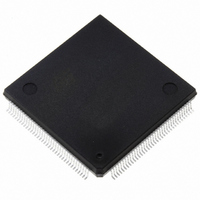
ST10F272Z2Q3 STMicroelectronics, ST10F272Z2Q3 Datasheet - Page 153

ST10F272Z2Q3
Manufacturer Part Number
ST10F272Z2Q3
Description
MCU 16BIT 256KB FLASH 144-PQFP
Manufacturer
STMicroelectronics
Series
ST10r
Datasheet
1.ST10F272Z2Q3.pdf
(189 pages)
Specifications of ST10F272Z2Q3
Core Processor
ST10
Core Size
16-Bit
Speed
64MHz
Connectivity
ASC, CAN, EBI/EMI, I²C, SSC, UART/USART
Peripherals
POR, PWM, WDT
Number Of I /o
111
Program Memory Size
256KB (256K x 8)
Program Memory Type
FLASH
Ram Size
20K x 8
Voltage - Supply (vcc/vdd)
4.5 V ~ 5.5 V
Data Converters
A/D 24x10b
Oscillator Type
Internal
Operating Temperature
-40°C ~ 125°C
Package / Case
144-QFP
Lead Free Status / RoHS Status
Lead free / RoHS Compliant
Eeprom Size
-
Other names
497-5579
Available stocks
Company
Part Number
Manufacturer
Quantity
Price
Company:
Part Number:
ST10F272Z2Q3
Manufacturer:
E-CMOS
Quantity:
10 000
Company:
Part Number:
ST10F272Z2Q3
Manufacturer:
STMicroelectronics
Quantity:
10 000
- Current page: 153 of 189
- Download datasheet (4Mb)
ST10F272Z2
Figure 45. Anti-aliasing filter and conversion rate
The considerations above lead to impose new constraints to the external circuit, to reduce
the accuracy error due to the voltage drop on C
above, it is simple to derive the following relation between the ideal and real sampled
voltage on C
From this formula, in the worst case (when V
assuming to accept a maximum error of half a count (~2.44mV), it is immediately evident a
constraints on C
In the next section an example of how to design the external network is provided, assuming
some reasonable values for the internal parameters and making hypothesis on the
characteristics of the analog signal to be sampled.
Example of external network sizing
The following hypothesis are formulated in order to proceed in designing the external
network on A/D Converter input pins:
●
●
●
●
●
●
●
●
●
●
●
Anti-Aliasing Filter (f
Analog Source Bandwidth (V
Analog Signal Source Bandwidth (f
conversion Rate (f
Sampling Time (T
Pin Input Capacitance (C
Pin Input Routing Capacitance (C
Sampling Capacitance (C
Maximum Input Current Injection (I
Maximum Analog Source Voltage (V
Analog Source Impedance (R
Channel Switch Resistance (R
Sampling Switch Resistance (R
S
:
f
f
0
F
F
value:
F
= RC Filter pole)
Noise
S
C
):1 µs
):25 kHz
f
f
A
P1
)
S
-----------
V A2
):4 pF
):5 pF
V A
S
SW
):100 Ω
AD
=
Sampled Signal Spectrum (f
):500 Ω
P2
------------------------------------------------------------
C P1
):200 Ω
C F 2048 C S
T
f
2 f
INJ
F
0
C
):1 pF
):10 kHz
AM)
= f
0
C P1
≤ 2 R
):3 mA
>
≤ f
0
+
:12 V
A
(Anti-aliasing Filtering Condition)
C
C P2
f
0
+
is maximum, that is for instance 5 V),
(Nyquist)
F
S
C P2
C
; from the two charge balance equations
⋅
F
+
(Conversion Rate vs. Filter Pole)
C F
+
C F
+
C S
f
C
C
= conversion Rate)
Electrical characteristics
f
153/189
Related parts for ST10F272Z2Q3
Image
Part Number
Description
Manufacturer
Datasheet
Request
R

Part Number:
Description:
STMicroelectronics [RIPPLE-CARRY BINARY COUNTER/DIVIDERS]
Manufacturer:
STMicroelectronics
Datasheet:

Part Number:
Description:
STMicroelectronics [LIQUID-CRYSTAL DISPLAY DRIVERS]
Manufacturer:
STMicroelectronics
Datasheet:

Part Number:
Description:
BOARD EVAL FOR MEMS SENSORS
Manufacturer:
STMicroelectronics
Datasheet:

Part Number:
Description:
NPN TRANSISTOR POWER MODULE
Manufacturer:
STMicroelectronics
Datasheet:

Part Number:
Description:
TURBOSWITCH ULTRA-FAST HIGH VOLTAGE DIODE
Manufacturer:
STMicroelectronics
Datasheet:

Part Number:
Description:
Manufacturer:
STMicroelectronics
Datasheet:

Part Number:
Description:
DIODE / SCR MODULE
Manufacturer:
STMicroelectronics
Datasheet:

Part Number:
Description:
DIODE / SCR MODULE
Manufacturer:
STMicroelectronics
Datasheet:

Part Number:
Description:
Search -----> STE16N100
Manufacturer:
STMicroelectronics
Datasheet:

Part Number:
Description:
Search ---> STE53NA50
Manufacturer:
STMicroelectronics
Datasheet:

Part Number:
Description:
NPN Transistor Power Module
Manufacturer:
STMicroelectronics
Datasheet:


