MC56F8002VWL Freescale Semiconductor, MC56F8002VWL Datasheet - Page 25
MC56F8002VWL
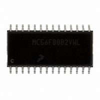
Manufacturer Part Number
MC56F8002VWL
Description
DSC 12K FLASH 32MHZ 28-SOIC
Manufacturer
Freescale Semiconductor
Series
56F8xxxr
Datasheet
1.MC56F8006DEMO.pdf
(100 pages)
Specifications of MC56F8002VWL
Core Processor
56800
Core Size
16-Bit
Speed
32MHz
Connectivity
I²C, LIN, SCI, SPI
Peripherals
LVD, POR, PWM, WDT
Number Of I /o
23
Program Memory Size
12KB (6K x 16)
Program Memory Type
FLASH
Ram Size
1K x 16
Voltage - Supply (vcc/vdd)
1.8 V ~ 3.6 V
Data Converters
A/D 15x12b
Oscillator Type
Internal
Operating Temperature
-40°C ~ 105°C
Package / Case
28-SOIC
Product
DSCs
Data Bus Width
16 bit
Processor Series
MC56F80xx
Core
56800E
Instruction Set Architecture
Dual Harvard
Device Million Instructions Per Second
32 MIPs
Maximum Clock Frequency
32 MHz
Number Of Programmable I/os
40
Data Ram Size
2 KB
Operating Supply Voltage
1.8 V to 3.6 V
Maximum Operating Temperature
+ 105 C
Mounting Style
SMD/SMT
Development Tools By Supplier
MC56F8006DEMO, APMOTOR56F8000E
Interface Type
LIN, I2C, SCI, SPI
Minimum Operating Temperature
- 40 C
For Use With
APMOTOR56F8000E - KIT DEMO MOTOR CTRL SYSTEM
Lead Free Status / RoHS Status
Lead free / RoHS Compliant
Eeprom Size
-
Lead Free Status / Rohs Status
Lead free / RoHS Compliant
Available stocks
Company
Part Number
Manufacturer
Quantity
Price

Part Number:
MC56F8002VWL
Manufacturer:
FREESCALE
Quantity:
20 000


Freescale Semiconductor
(ANA4 and
CMP1_P2)
(GPIOD0)
(GPIOD1)
(GPIOD2)
(ANB12)
(ANB10)
(CMP0_
(CMP2_
(CMP2_
Signal
(TIN2)
Name
OUT)
OUT)
OUT)
TDO
(SS)
TCK
(T0)
TDI
SOIC
28
23
25
9
LQFP
Table 5. 56F8006/56F8002 Signal and Package Information (continued)
32
30
32
14
LQFP
48
45
48
22
MC56F8006/MC56F8002 Digital Signal Controller, Rev. 3
Output
Analog
Output
Output
Output
Analog
Output
Output
Output
Analog
Output
Input/
Input/
Input/
Input/
Type
Input
Input
Input
Input
Input
Input
Input
tri-stated,
enabled
enabled
enabled
internal
Output,
internal
internal
During
Reset
pullup
pullup
pullup
Input,
Input,
State
Test Data Input — This input pin provides a serial input data stream
to the JTAG/EOnCE port. It is sampled on the rising edge of TCK
and has an on-chip pullup resistor.
Port D GPIO — This GPIO pin can be individually programmed as
an input or output pin.
ANB12 — Analog input to channel 12 of ADCB
SS — SS is used in slave mode to indicate to the SPI module that
the current transfer is to be received.
TIN2 — Dual timer module channel 2 input.
CMP1_OUT — Analog comparator 1 output.
After reset, the default state is TDI.
Test Data Output — This three-stateable output pin provides a serial
output data stream from the JTAG/EOnCE port. It is driven in the
shift-IR and shift-DR controller states, and changes on the falling
edge of TCK.
Port D GPIO — This GPIO pin can be individually programmed as
an input or output pin.
ANB10 — Analog input to channel 10 of ADCB.
T0 — Dual timer module channel 0 input/output.
CMP2_OUT — Analog comparator 2 output.
After reset, the default state is TDO.
Test Clock Input — This input pin provides a gated clock to
synchronize the test logic and shift serial data to the JTAG/EOnCE
port. The pin is connected internally to a pullup resistor. A
Schmitt-trigger input is used for noise immunity.
Port D GPIO — This GPIO pin can be individually programmed as
an input or output pin.
ANA4 and CMP1_P2 — Analog input to channel 4 of ADCA and
positive input 2 of analog comparator 1.
CMP2_OUT — Analog comparator 2 output.
After reset, the default state is TCK.
Signal Description
Signal/Connection Descriptions
25
Related parts for MC56F8002VWL
Image
Part Number
Description
Manufacturer
Datasheet
Request
R

Part Number:
Description:
Manufacturer:
Freescale Semiconductor, Inc
Datasheet:
Part Number:
Description:
Manufacturer:
Freescale Semiconductor, Inc
Datasheet:
Part Number:
Description:
Manufacturer:
Freescale Semiconductor, Inc
Datasheet:
Part Number:
Description:
Manufacturer:
Freescale Semiconductor, Inc
Datasheet:
Part Number:
Description:
Manufacturer:
Freescale Semiconductor, Inc
Datasheet:
Part Number:
Description:
Manufacturer:
Freescale Semiconductor, Inc
Datasheet:
Part Number:
Description:
Manufacturer:
Freescale Semiconductor, Inc
Datasheet:
Part Number:
Description:
Manufacturer:
Freescale Semiconductor, Inc
Datasheet:
Part Number:
Description:
Manufacturer:
Freescale Semiconductor, Inc
Datasheet:
Part Number:
Description:
Manufacturer:
Freescale Semiconductor, Inc
Datasheet:
Part Number:
Description:
Manufacturer:
Freescale Semiconductor, Inc
Datasheet:
Part Number:
Description:
Manufacturer:
Freescale Semiconductor, Inc
Datasheet:
Part Number:
Description:
Manufacturer:
Freescale Semiconductor, Inc
Datasheet:
Part Number:
Description:
Manufacturer:
Freescale Semiconductor, Inc
Datasheet:
Part Number:
Description:
Manufacturer:
Freescale Semiconductor, Inc
Datasheet: