MC56F8002VWL Freescale Semiconductor, MC56F8002VWL Datasheet - Page 44
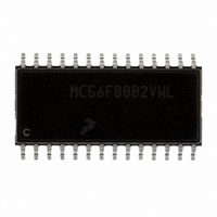
MC56F8002VWL
Manufacturer Part Number
MC56F8002VWL
Description
DSC 12K FLASH 32MHZ 28-SOIC
Manufacturer
Freescale Semiconductor
Series
56F8xxxr
Datasheet
1.MC56F8006DEMO.pdf
(100 pages)
Specifications of MC56F8002VWL
Core Processor
56800
Core Size
16-Bit
Speed
32MHz
Connectivity
I²C, LIN, SCI, SPI
Peripherals
LVD, POR, PWM, WDT
Number Of I /o
23
Program Memory Size
12KB (6K x 16)
Program Memory Type
FLASH
Ram Size
1K x 16
Voltage - Supply (vcc/vdd)
1.8 V ~ 3.6 V
Data Converters
A/D 15x12b
Oscillator Type
Internal
Operating Temperature
-40°C ~ 105°C
Package / Case
28-SOIC
Product
DSCs
Data Bus Width
16 bit
Processor Series
MC56F80xx
Core
56800E
Instruction Set Architecture
Dual Harvard
Device Million Instructions Per Second
32 MIPs
Maximum Clock Frequency
32 MHz
Number Of Programmable I/os
40
Data Ram Size
2 KB
Operating Supply Voltage
1.8 V to 3.6 V
Maximum Operating Temperature
+ 105 C
Mounting Style
SMD/SMT
Development Tools By Supplier
MC56F8006DEMO, APMOTOR56F8000E
Interface Type
LIN, I2C, SCI, SPI
Minimum Operating Temperature
- 40 C
For Use With
APMOTOR56F8000E - KIT DEMO MOTOR CTRL SYSTEM
Lead Free Status / RoHS Status
Lead free / RoHS Compliant
Eeprom Size
-
Lead Free Status / Rohs Status
Lead free / RoHS Compliant
Available stocks
Company
Part Number
Manufacturer
Quantity
Price

Part Number:
MC56F8002VWL
Manufacturer:
FREESCALE
Quantity:
20 000


Specifications
8.4
This section includes information about recommended operating conditions.
44
Ambient Operating Temperature (Extended
Output Source Current Low (at V
Output Source Current High at V
When programmed for high drive strength
When programmed for high drive strength
When programmed for low drive strength
When programmed for low drive strength
XTAL driven by an external clock source
Input Voltage High (digital inputs)
Input Voltage Low (digital inputs)
Flash Data Retention with <100
Voltage difference V
Voltage difference V
Oscillator Input Voltage High
Oscillator Input Voltage Low
Using external clock source
Using relaxation oscillator
Device Clock Frequency
(Program Erase Cycles)
Program/Erase Cycles
Recommended Operating Conditions
Flash Data Retention
Flash Endurance
Characteristic
Supply voltage
Industrial)
Junction-to-board thermal resistance determined per JEDEC JESD51–8. Thermal test
board meets JEDEC specification for the specified package.
Junction-to-case at the top of the package determined using MIL-STD 883 Method 1012.1.
The cold plate temperature is used for the case temperature. Reported value includes the
thermal resistance of the interface layer.
Thermal characterization parameter indicating the temperature difference between the
package top and the junction temperature per JEDEC JESD51–2. When Greek letters are
not available, the thermal characterization parameter is written as Psi-JT
Junction temperature is a function of die size, on-chip power dissipation, package thermal
resistance, mounting site (board) temperature, ambient temperature, air flow, power
dissipation of other components on the board, and board thermal resistance.
See
considerations.
Section 9.1, “Thermal Design
DD
SS
to V
to V
MC56F8006/MC56F8002 Digital Signal Controller, Rev. 3
OL
SSA
OH
DDA
Table 18. Recommended Operating Conditions
max.)
min.)
(V
1
1
REFL x
V
FSYSCLK
Symbol
DD,
V
V
t
FLRET
IHOSC
ILOSC
V
I
V
V
I
V
N
T
OH
t
OL
= 0 V, V
R
V
IH
DD
IL
A
SS
F
Considerations,” for more detail on thermal design
DDA
T
SSA
A
Pin Groups 1, 2
Pin Groups 1, 2
Pin Groups 1, 2
Pin Groups 1, 2
= –40°C to 125°C
T
T
Pin Group 4
Pin Group 4
Pin Group 1
Pin Group 1
J
J
= 0 V, V
Notes
85°C avg
85°C avg
SS
= 0 V)
10,000
–0.1
–0.1
–0.3
–0.3
Min
–40
2.0
2.0
15
20
—
—
—
—
3
1
0
Typ
3.3
—
0
0
Freescale Semiconductor
V
DDA
Max
V
105
3.6
0.1
0.1
0.8
0.8
32
32
–4
–8
—
—
—
4
8
DD
+ 0.3
cycles
years
years
Unit
MHz
mA
mA
°C
V
V
V
V
V
V
V
Related parts for MC56F8002VWL
Image
Part Number
Description
Manufacturer
Datasheet
Request
R

Part Number:
Description:
Manufacturer:
Freescale Semiconductor, Inc
Datasheet:
Part Number:
Description:
Manufacturer:
Freescale Semiconductor, Inc
Datasheet:
Part Number:
Description:
Manufacturer:
Freescale Semiconductor, Inc
Datasheet:
Part Number:
Description:
Manufacturer:
Freescale Semiconductor, Inc
Datasheet:
Part Number:
Description:
Manufacturer:
Freescale Semiconductor, Inc
Datasheet:
Part Number:
Description:
Manufacturer:
Freescale Semiconductor, Inc
Datasheet:
Part Number:
Description:
Manufacturer:
Freescale Semiconductor, Inc
Datasheet:
Part Number:
Description:
Manufacturer:
Freescale Semiconductor, Inc
Datasheet:
Part Number:
Description:
Manufacturer:
Freescale Semiconductor, Inc
Datasheet:
Part Number:
Description:
Manufacturer:
Freescale Semiconductor, Inc
Datasheet:
Part Number:
Description:
Manufacturer:
Freescale Semiconductor, Inc
Datasheet:
Part Number:
Description:
Manufacturer:
Freescale Semiconductor, Inc
Datasheet:
Part Number:
Description:
Manufacturer:
Freescale Semiconductor, Inc
Datasheet:
Part Number:
Description:
Manufacturer:
Freescale Semiconductor, Inc
Datasheet:
Part Number:
Description:
Manufacturer:
Freescale Semiconductor, Inc
Datasheet: