MC56F8002VWL Freescale Semiconductor, MC56F8002VWL Datasheet - Page 38
MC56F8002VWL
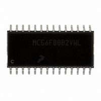
Manufacturer Part Number
MC56F8002VWL
Description
DSC 12K FLASH 32MHZ 28-SOIC
Manufacturer
Freescale Semiconductor
Series
56F8xxxr
Datasheet
1.MC56F8006DEMO.pdf
(100 pages)
Specifications of MC56F8002VWL
Core Processor
56800
Core Size
16-Bit
Speed
32MHz
Connectivity
I²C, LIN, SCI, SPI
Peripherals
LVD, POR, PWM, WDT
Number Of I /o
23
Program Memory Size
12KB (6K x 16)
Program Memory Type
FLASH
Ram Size
1K x 16
Voltage - Supply (vcc/vdd)
1.8 V ~ 3.6 V
Data Converters
A/D 15x12b
Oscillator Type
Internal
Operating Temperature
-40°C ~ 105°C
Package / Case
28-SOIC
Product
DSCs
Data Bus Width
16 bit
Processor Series
MC56F80xx
Core
56800E
Instruction Set Architecture
Dual Harvard
Device Million Instructions Per Second
32 MIPs
Maximum Clock Frequency
32 MHz
Number Of Programmable I/os
40
Data Ram Size
2 KB
Operating Supply Voltage
1.8 V to 3.6 V
Maximum Operating Temperature
+ 105 C
Mounting Style
SMD/SMT
Development Tools By Supplier
MC56F8006DEMO, APMOTOR56F8000E
Interface Type
LIN, I2C, SCI, SPI
Minimum Operating Temperature
- 40 C
For Use With
APMOTOR56F8000E - KIT DEMO MOTOR CTRL SYSTEM
Lead Free Status / RoHS Status
Lead free / RoHS Compliant
Eeprom Size
-
Lead Free Status / Rohs Status
Lead free / RoHS Compliant
Available stocks
Company
Part Number
Manufacturer
Quantity
Price

Part Number:
MC56F8002VWL
Manufacturer:
FREESCALE
Quantity:
20 000


Security Features
Each ADC contains a temperature sensor. Outputs of temperature sensors, PGAs, on-chip regulators and VDDA are internally
routed to ADC inputs.
6.8
The DSP56800E Family includes extensive integrated support for application software development and real-time debugging.
Two modules, the Enhanced On-Chip Emulation module (EOnCE) and the core test access port (TAP, commonly called the
JTAG port), work together to provide these capabilities. Both are accessed through a common 4-pin JTAG/EOnCE interface.
These modules allow you to insert the 56F8006/56F8002 into a target system while retaining debug control. This capability is
especially important for devices without an external bus, because it eliminates the need for a costly cable to bring out the
footprint of the chip, as is required by a traditional emulator system.
The DSP56800E EOnCE module is a Freescale-designed module used to develop and debug application software used with the
chip. This module allows non-intrusive interaction with the CPU and is accessible through the pins of the JTAG interface or by
software program control of the DSP56800E core. Among the many features of the EOnCE module is the support for data
communication between the controller and the host software development and debug systems in real-time program execution.
Other features allow for hardware breakpoints, the monitoring and tracking of program execution, and the ability to examine
and modify the contents of registers, memory, and on-chip peripherals, all in a special debug environment. No user-accessible
resources need to be sacrificed to perform debugging operations.
The DSP56800E JTAG port is used to provide an interface for the EOnCE module to the DSP JTAG pins. Joint Test Action
Group (JTAG) boundary scan is an IEEE 1149.1 standard methodology enabling access to test features using a test access port
(TAP). A JTAG boundary scan consists of a TAP controller and boundary scan registers. Please contact your Freescale sales
representative or authorized distributor for device-specific BSDL information.
7
The 56F8006/56F8002 offers security features intended to prevent unauthorized users from reading the contents of the flash
memory (FM) array. The 56F8006/56F8002’s flash security consists of several hardware interlocks that prevent unauthorized
users from gaining access to the flash array.
After flash security is set, an authorized user can be enabled to access on-chip memory if a user-defined software subroutine,
which reads and transfers the contents of internal memory via peripherals, is included in the application software. This
38
•
•
•
•
•
•
•
•
•
•
•
•
•
Internal PGA0 output available on ANA15
Internal PGA0 positive input calibration voltage available on ANA16
Internal PGA0 negative input calibration voltage available on ANA17
Internal PGA1 output available on ANB15
Internal PGA1 positive input calibration voltage available on ANB16
Internal PGA1 negative input calibration voltage available on ANB17
ADCA temperature sensor available on ANA26
ADCB temperature sensor available on ANB26
Output of on-chip digital voltage regulator is routed to ANA24
Output of on-chip analog voltage regulator is routed to ANA25
Output of on-chip small voltage regulator for ROSC is routed to ANB24
Output of on-chip small voltage regulator for PLL is routed to ANB25
VDDA is routed to ANA27 and ANB27
Joint Test Action Group (JTAG)/Enhanced On-Chip Emulator
(EOnCE)
Security Features
In normal operation, an external pullup on the TMS pin is highly recommend to place the
JTAG state machine in reset state if this pin is not configured as GPIO.
MC56F8006/MC56F8002 Digital Signal Controller, Rev. 3
NOTE
Freescale Semiconductor
Related parts for MC56F8002VWL
Image
Part Number
Description
Manufacturer
Datasheet
Request
R

Part Number:
Description:
Manufacturer:
Freescale Semiconductor, Inc
Datasheet:
Part Number:
Description:
Manufacturer:
Freescale Semiconductor, Inc
Datasheet:
Part Number:
Description:
Manufacturer:
Freescale Semiconductor, Inc
Datasheet:
Part Number:
Description:
Manufacturer:
Freescale Semiconductor, Inc
Datasheet:
Part Number:
Description:
Manufacturer:
Freescale Semiconductor, Inc
Datasheet:
Part Number:
Description:
Manufacturer:
Freescale Semiconductor, Inc
Datasheet:
Part Number:
Description:
Manufacturer:
Freescale Semiconductor, Inc
Datasheet:
Part Number:
Description:
Manufacturer:
Freescale Semiconductor, Inc
Datasheet:
Part Number:
Description:
Manufacturer:
Freescale Semiconductor, Inc
Datasheet:
Part Number:
Description:
Manufacturer:
Freescale Semiconductor, Inc
Datasheet:
Part Number:
Description:
Manufacturer:
Freescale Semiconductor, Inc
Datasheet:
Part Number:
Description:
Manufacturer:
Freescale Semiconductor, Inc
Datasheet:
Part Number:
Description:
Manufacturer:
Freescale Semiconductor, Inc
Datasheet:
Part Number:
Description:
Manufacturer:
Freescale Semiconductor, Inc
Datasheet:
Part Number:
Description:
Manufacturer:
Freescale Semiconductor, Inc
Datasheet: