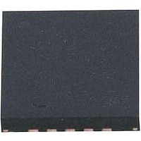
ATTINY25-15MZ Atmel, ATTINY25-15MZ Datasheet - Page 86

ATTINY25-15MZ
Manufacturer Part Number
ATTINY25-15MZ
Description
MCU AVR 2K FLASH 15MHZ 20-QFN
Manufacturer
Atmel
Series
AVR® ATtinyr
Datasheet
1.ATTINY25-15MZ.pdf
(196 pages)
Specifications of ATTINY25-15MZ
Package / Case
20-QFN
Voltage - Supply (vcc/vdd)
2.7 V ~ 5.5 V
Operating Temperature
-40°C ~ 125°C
Speed
16MHz
Number Of I /o
6
Eeprom Size
128 x 8
Core Processor
AVR
Program Memory Type
FLASH
Ram Size
128 x 8
Program Memory Size
2KB (2K x 8)
Data Converters
A/D 4x10b
Oscillator Type
Internal
Peripherals
Brown-out Detect/Reset, POR, PWM, WDT
Connectivity
USI
Core Size
8-Bit
Processor Series
ATTINY2x
Core
AVR8
Data Bus Width
8 bit
Data Ram Size
128 B
Interface Type
UART, SPI, USI
Maximum Clock Frequency
16 MHz
Number Of Programmable I/os
6
Number Of Timers
2
Maximum Operating Temperature
+ 85 C
Mounting Style
SMD/SMT
3rd Party Development Tools
EWAVR, EWAVR-BL
Development Tools By Supplier
ATAVRDRAGON, ATSTK500, ATSTK600, ATAVRISP2, ATAVRONEKIT
Minimum Operating Temperature
- 40 C
On-chip Adc
10 bit, 4 Channel
Data Rom Size
128 B
A/d Bit Size
10 bit
A/d Channels Available
4
Height
0.75 mm
Length
4 mm
Supply Voltage (max)
5.5 V
Supply Voltage (min)
2.7 V
Width
4 mm
Lead Free Status / RoHS Status
Lead free / RoHS Compliant
- Current page: 86 of 196
- Download datasheet (4Mb)
14.1.3
14.1.4
86
ATtiny25/45/85
Timer/Counter1 - TCNT1
Timer/Counter1 Output Compare RegisterA - OCR1A
• Bit 3- FOC1B: Force Output Compare Match 1B
Writing a logical one to this bit forces a change in the compare match output pin PB3 (OC1B)
according to the values already set in COM1B1 and COM1B0. If COM1B1 and COM1B0 written
in the same cycle as FOC1B, the new settings will be used. The Force Output Compare bit can
be used to change the output pin value regardless of the timer value. The automatic action pro-
grammed in COM1B1 and COM1B0 takes place as if a compare match had occurred, but no
interrupt is generated. The FOC1B bit always reads as zero. FOC1B is not in use if PWM1B bit
is set.
• Bit 2- FOC1A: Force Output Compare Match 1A
Writing a logical one to this bit forces a change in the compare match output pin PB1 (OC1A)
according to the values already set in COM1A1 and COM1A0. If COM1A1 and COM1A0 written
in the same cycle as FOC1A, the new settings will be used. The Force Output Compare bit can
be used to change the output pin value regardless of the timer value. The automatic action pro-
grammed in COM1A1 and COM1A0 takes place as if a compare match had occurred, but no
interrupt is generated. The FOC1A bit always reads as zero. FOC1A is not in use if PWM1A bit
is set.
• Bit 1- PSR1 : Prescaler Reset Timer/Counter1
When this bit is set (one), the Timer/Counter prescaler (TCNT1 is unaffected) will be reset. The
bit will be cleared by hardware after the operation is performed. Writing a zero to this bit will have
no effect. This bit will always read as zero.
This 8-bit register contains the value of Timer/Counter1.
Timer/Counter1 is realized as an up counter with read and write access. Due to synchronization
of the CPU, Timer/Counter1 data written into Timer/Counter1 is delayed by one and half CPU
clock cycles in synchronous mode and at most one CPU clock cycles for asynchronous mode.
The output compare register A is an 8-bit read/write register.
The Timer/Counter Output Compare Register A contains data to be continuously compared with
Timer/Counter1. Actions on compare matches are specified in TCCR1. A compare match does
only occur if Timer/Counter1 counts to the OCR1A value. A software write that sets TCNT1 and
OCR1A to the same value does not generate a compare match.
A compare match will set the compare interrupt flag OCF1A after a synchronization delay follow-
ing the compare event.
Bit
$2F ($4F)
Read/Write
Initial value
Bit
$2E ($4E)
Read/Write
Initial value
MSB
MSB
R/W
R/W
7
0
7
0
R/W
R/W
6
0
6
0
R/W
R/W
5
0
5
0
R/W
R/W
4
0
4
0
R/W
R/W
3
0
3
0
R/W
R/W
2
0
2
0
R/W
R/W
1
0
1
0
LSB
R/W
LSB
R/W
0
0
0
0
7598H–AVR–07/09
OCR1A
TCNT1
Related parts for ATTINY25-15MZ
Image
Part Number
Description
Manufacturer
Datasheet
Request
R

Part Number:
Description:
Manufacturer:
Atmel Corporation
Datasheet:

Part Number:
Description:
Manufacturer:
Atmel Corporation
Datasheet:

Part Number:
Description:
IC MCU AVR 2K FLASH 20MHZ 20-QFN
Manufacturer:
Atmel
Datasheet:

Part Number:
Description:
IC AVR MCU 2K 20MHZ 8-DIP
Manufacturer:
Atmel
Datasheet:

Part Number:
Description:
IC AVR MCU 2K 20MHZ 8-SOIC
Manufacturer:
Atmel
Datasheet:

Part Number:
Description:
8-bit Microcontrollers - MCU AVR 16KB FL 512B EE 1KB SRAM 10 MHZ GRN
Manufacturer:
Atmel

Part Number:
Description:
8-bit Microcontrollers - MCU AVR 16KB FL 512B EE 1KB SRAM 10 MHZ GRN
Manufacturer:
Atmel

Part Number:
Description:
MCU AVR 2K ISP FLASH 2.7V 8-SOIC
Manufacturer:
Atmel
Datasheet:

Part Number:
Description:
MCU AVR 2KB FLASH 20MHZ 8SOIC
Manufacturer:
Atmel
Datasheet:

Part Number:
Description:
IC MCU AVR 2KB FLASH 20MHZ 8SOIC
Manufacturer:
Atmel
Datasheet:

Part Number:
Description:
IC MCU AVR 2KB FLASH 20MHZ 8SOIC
Manufacturer:
Atmel
Datasheet:

Part Number:
Description:
MCU AVR 2KB FLASH 20MHZ 8SOIC
Manufacturer:
Atmel
Datasheet:

Part Number:
Description:
MCU AVR 2KB FLASH 20MHZ 8SOIC
Manufacturer:
Atmel
Datasheet:

Part Number:
Description:
MCU AVR 2KB FLASH 20MHZ 20QFN
Manufacturer:
Atmel
Datasheet:


