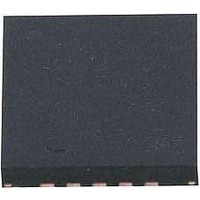
ATTINY25-15MZ Atmel, ATTINY25-15MZ Datasheet - Page 98

ATTINY25-15MZ
Manufacturer Part Number
ATTINY25-15MZ
Description
MCU AVR 2K FLASH 15MHZ 20-QFN
Manufacturer
Atmel
Series
AVR® ATtinyr
Datasheet
1.ATTINY25-15MZ.pdf
(196 pages)
Specifications of ATTINY25-15MZ
Package / Case
20-QFN
Voltage - Supply (vcc/vdd)
2.7 V ~ 5.5 V
Operating Temperature
-40°C ~ 125°C
Speed
16MHz
Number Of I /o
6
Eeprom Size
128 x 8
Core Processor
AVR
Program Memory Type
FLASH
Ram Size
128 x 8
Program Memory Size
2KB (2K x 8)
Data Converters
A/D 4x10b
Oscillator Type
Internal
Peripherals
Brown-out Detect/Reset, POR, PWM, WDT
Connectivity
USI
Core Size
8-Bit
Processor Series
ATTINY2x
Core
AVR8
Data Bus Width
8 bit
Data Ram Size
128 B
Interface Type
UART, SPI, USI
Maximum Clock Frequency
16 MHz
Number Of Programmable I/os
6
Number Of Timers
2
Maximum Operating Temperature
+ 85 C
Mounting Style
SMD/SMT
3rd Party Development Tools
EWAVR, EWAVR-BL
Development Tools By Supplier
ATAVRDRAGON, ATSTK500, ATSTK600, ATAVRISP2, ATAVRONEKIT
Minimum Operating Temperature
- 40 C
On-chip Adc
10 bit, 4 Channel
Data Rom Size
128 B
A/d Bit Size
10 bit
A/d Channels Available
4
Height
0.75 mm
Length
4 mm
Supply Voltage (max)
5.5 V
Supply Voltage (min)
2.7 V
Width
4 mm
Lead Free Status / RoHS Status
Lead free / RoHS Compliant
- Current page: 98 of 196
- Download datasheet (4Mb)
16.2.2
98
ATtiny25/45/85
SPI Master Operation Example
Figure 16-3. Three-wire Mode, Timing Diagram
The Three-wire mode timing is shown in Figure 16-3. At the top of the figure is a USCK cycle ref-
erence. One bit is shifted into the USI Shift Register (USIDR) for each of these cycles. The
USCK timing is shown for both external clock modes. In External Clock mode 0 (USICS0 = 0), DI
is sampled at positive edges, and DO is changed (Data Register is shifted by one) at negative
edges. External Clock mode 1 (USICS0 = 1) uses the opposite edges versus mode 0, i.e., sam-
ples data at negative and changes the output at positive edges. The USI clock modes
corresponds to the SPI data mode 0 and 1.
Referring to the timing diagram (Figure 16-3.), a bus transfer involves the following steps:
The following code demonstrates how to use the USI module as a SPI Master:
1. The Slave device and Master device sets up its data output and, depending on the pro-
2. The Master generates a clock pulse by software toggling the USCK line twice (C and
3. Step 2. is repeated eight times for a complete register (byte) transfer.
4. After eight clock pulses (i.e., 16 clock edges) the counter will overflow and indicate that
SPITransfer:
SPITransfer_loop:
CYCLE
tocol used, enables its output driver (mark A and B). The output is set up by writing the
data to be transmitted to the Serial Data Register. Enabling of the output is done by set-
ting the corresponding bit in the port Data Direction Register. Note that point A and B
does not have any specific order, but both must be at least one half USCK cycle before
point C where the data is sampled. This must be done to ensure that the data setup
requirement is satisfied. The 4-bit counter is reset to zero.
D). The bit value on the slave and master’s data input (DI) pin is sampled by the USI on
the first edge (C), and the data output is changed on the opposite edge (D). The 4-bit
counter will count both edges.
the transfer is completed. The data bytes transferred must now be processed before a
new transfer can be initiated. The overflow interrupt will wake up the processor if it is set
to Idle mode. Depending of the protocol used the slave device can now set its output to
high impedance.
USCK
USCK
sts
ldi
sts
ldi
sts
lds
sbrs
DO
DI
( Reference )
A
USIDR,r16
r16,(1<<USIOIF)
USISR,r16
r16,(1<<USIWM0)|(1<<USICS1)|(1<<USICLK)|(1<<USITC)
USICR,r16
r16, USISR
r16, USIOIF
B
MSB
MSB
C
1
D
2
6
6
3
5
5
4
4
4
5
3
3
6
2
2
7
1
1
LSB
LSB
8
7598H–AVR–07/09
E
Related parts for ATTINY25-15MZ
Image
Part Number
Description
Manufacturer
Datasheet
Request
R

Part Number:
Description:
Manufacturer:
Atmel Corporation
Datasheet:

Part Number:
Description:
Manufacturer:
Atmel Corporation
Datasheet:

Part Number:
Description:
IC MCU AVR 2K FLASH 20MHZ 20-QFN
Manufacturer:
Atmel
Datasheet:

Part Number:
Description:
IC AVR MCU 2K 20MHZ 8-DIP
Manufacturer:
Atmel
Datasheet:

Part Number:
Description:
IC AVR MCU 2K 20MHZ 8-SOIC
Manufacturer:
Atmel
Datasheet:

Part Number:
Description:
8-bit Microcontrollers - MCU AVR 16KB FL 512B EE 1KB SRAM 10 MHZ GRN
Manufacturer:
Atmel

Part Number:
Description:
8-bit Microcontrollers - MCU AVR 16KB FL 512B EE 1KB SRAM 10 MHZ GRN
Manufacturer:
Atmel

Part Number:
Description:
MCU AVR 2K ISP FLASH 2.7V 8-SOIC
Manufacturer:
Atmel
Datasheet:

Part Number:
Description:
MCU AVR 2KB FLASH 20MHZ 8SOIC
Manufacturer:
Atmel
Datasheet:

Part Number:
Description:
IC MCU AVR 2KB FLASH 20MHZ 8SOIC
Manufacturer:
Atmel
Datasheet:

Part Number:
Description:
IC MCU AVR 2KB FLASH 20MHZ 8SOIC
Manufacturer:
Atmel
Datasheet:

Part Number:
Description:
MCU AVR 2KB FLASH 20MHZ 8SOIC
Manufacturer:
Atmel
Datasheet:

Part Number:
Description:
MCU AVR 2KB FLASH 20MHZ 8SOIC
Manufacturer:
Atmel
Datasheet:

Part Number:
Description:
MCU AVR 2KB FLASH 20MHZ 20QFN
Manufacturer:
Atmel
Datasheet:


