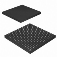
AT91SAM9G45-CU-999 Atmel, AT91SAM9G45-CU-999 Datasheet - Page 613

AT91SAM9G45-CU-999
Manufacturer Part Number
AT91SAM9G45-CU-999
Description
IC MCU ARM9 APMC 324TFBGA
Manufacturer
Atmel
Series
AT91SAMr
Datasheet
1.AT91SAM9G45-EKES.pdf
(1218 pages)
Specifications of AT91SAM9G45-CU-999
Core Processor
ARM9
Core Size
16/32-Bit
Speed
400MHz
Connectivity
EBI/EMI, Ethernet, I²C, IrDA, MMC, SPI, SSC, UART/USART, USB
Peripherals
AC'97, DMA, I²S, LCD, POR, PWM, WDT
Number Of I /o
160
Program Memory Size
64KB (64K x 8)
Program Memory Type
ROM
Ram Size
128K x 8
Voltage - Supply (vcc/vdd)
0.9 V ~ 1.1 V
Data Converters
A/D 8x10b
Oscillator Type
Internal
Operating Temperature
-40°C ~ 85°C
Package / Case
324-TFBGA
Lead Free Status / RoHS Status
Lead free / RoHS Compliant
Eeprom Size
-
Lead Free Status / Rohs Status
Supplier Unconfirmed
Available stocks
Company
Part Number
Manufacturer
Quantity
Price
- Current page: 613 of 1218
- Download datasheet (19Mb)
33.7.8.23
Figure 33-52. Master Node with PDC (PDCM=1)
6438F–ATARM–21-Jun-10
WRITE BUFFER
IDENTIFIER
CHKTYP
CHKDIS
PARDIS
DATA N
DATA 0
FSDIS
NACT
DLM
DLC
|
|
|
|
Master Node Configuration
(DMA)
PDC
The PDC uses the trigger flags, TXRDY and RXRDY, to write or read into the USART. The PDC
always writes in the Transmit Holding register (US_THR) and it always reads in the Receive
Holding register (US_RHR). The size of the data written or read by the PDC in the USART is
always a byte.
The user can choose between two PDC modes by the PDCM bit in the LIN Mode register
(US_LINMR):
The WRITE buffer also contains the Identifier and the DATA, if the USART sends the response
(NACT = PUBLISH).
The READ buffer contains the DATA if the USART receives the response (NACT =
SUBSCRIBE).
• PDCM = 1: the LIN configuration is stored in the WRITE buffer and it is written by the PDC in
• PDCM = 0: the LIN configuration is not stored in the WRITE buffer and it must be written by
the Transmit Holding register US_THR (instead of the LIN Mode register US_LINMR).
Because the PDC transfer size is limited to a byte, the transfer is split into two accesses.
During the first access the bits, NACT, PARDIS, CHKDIS, CHKTYP, DLM and FDIS are
written. During the second access the 8-bit DLC field is written.
the user in the LIN Mode register (US_LINMR).
APB bus
RXRDY
NODE ACTION = PUBLISH
LIN CONTROLLER
USART3
WRITE BUFFER
READ BUFFER
IDENTIFIER
CHKTYP
PARDIS
CHKDIS
DATA N
DATA 0
FSDIS
NACT
DLM
DLC
|
|
|
|
(DMA)
PDC
AT91SAM9G45
APB bus
RXRDY
TXRDY
NODE ACTION = SUBSCRIBE
LIN CONTROLLER
USART3
613
Related parts for AT91SAM9G45-CU-999
Image
Part Number
Description
Manufacturer
Datasheet
Request
R

Part Number:
Description:
KIT EVAL FOR AT91SAM9G45
Manufacturer:
Atmel
Datasheet:

Part Number:
Description:
MCU ARM9 324-TFBGA
Manufacturer:
Atmel
Datasheet:

Part Number:
Description:
At91 Arm Thumb-based Microcontrollers
Manufacturer:
ATMEL Corporation
Datasheet:

Part Number:
Description:
MCU, MPU & DSP Development Tools KICKSTART KIT FOR AT91SAM9 PLUS
Manufacturer:
IAR Systems

Part Number:
Description:
DEV KIT FOR AVR/AVR32
Manufacturer:
Atmel
Datasheet:

Part Number:
Description:
INTERVAL AND WIPE/WASH WIPER CONTROL IC WITH DELAY
Manufacturer:
ATMEL Corporation
Datasheet:

Part Number:
Description:
Low-Voltage Voice-Switched IC for Hands-Free Operation
Manufacturer:
ATMEL Corporation
Datasheet:

Part Number:
Description:
MONOLITHIC INTEGRATED FEATUREPHONE CIRCUIT
Manufacturer:
ATMEL Corporation
Datasheet:

Part Number:
Description:
AM-FM Receiver IC U4255BM-M
Manufacturer:
ATMEL Corporation
Datasheet:

Part Number:
Description:
Monolithic Integrated Feature Phone Circuit
Manufacturer:
ATMEL Corporation
Datasheet:

Part Number:
Description:
Multistandard Video-IF and Quasi Parallel Sound Processing
Manufacturer:
ATMEL Corporation
Datasheet:

Part Number:
Description:
High-performance EE PLD
Manufacturer:
ATMEL Corporation
Datasheet:


