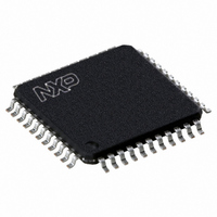
P89CV51RD2FBC,557 NXP Semiconductors, P89CV51RD2FBC,557 Datasheet - Page 59

P89CV51RD2FBC,557
Manufacturer Part Number
P89CV51RD2FBC,557
Description
IC 80C51 MCU FLASH 64K 44-TQFP
Manufacturer
NXP Semiconductors
Series
89Cr
Datasheet
1.P89CV51RB2FA512.pdf
(76 pages)
Specifications of P89CV51RD2FBC,557
Core Processor
8051
Core Size
8-Bit
Speed
40MHz
Connectivity
EBI/EMI, SPI, UART/USART
Peripherals
POR, PWM, WDT
Number Of I /o
32
Program Memory Size
64KB (64K x 8)
Program Memory Type
FLASH
Ram Size
1K x 8
Voltage - Supply (vcc/vdd)
4.5 V ~ 5.5 V
Oscillator Type
Internal
Operating Temperature
-40°C ~ 85°C
Package / Case
44-TQFP, 44-VQFP
Processor Series
P89CV5x
Core
80C51
Data Bus Width
8 bit
Data Ram Size
1 KB
Interface Type
SPI, UART
Maximum Clock Frequency
40 MHz
Number Of Programmable I/os
32
Number Of Timers
3
Operating Supply Voltage
4.5 V to 5.5 V
Maximum Operating Temperature
+ 85 C
Mounting Style
SMD/SMT
3rd Party Development Tools
PK51, CA51, A51, ULINK2
Minimum Operating Temperature
- 40 C
Cpu Family
89C
Device Core
80C51
Device Core Size
8b
Frequency (max)
40MHz
Total Internal Ram Size
1KB
# I/os (max)
32
Number Of Timers - General Purpose
3
Operating Supply Voltage (typ)
5V
Operating Supply Voltage (max)
5.5V
Operating Supply Voltage (min)
4.5V
Instruction Set Architecture
CISC
Operating Temp Range
-40C to 85C
Operating Temperature Classification
Industrial
Mounting
Surface Mount
Pin Count
44
Package Type
TQFP
Lead Free Status / RoHS Status
Lead free / RoHS Compliant
Eeprom Size
-
Data Converters
-
Lead Free Status / Rohs Status
Details
Other names
568-4257
935284103557
P89CV51RD2FBC
935284103557
P89CV51RD2FBC
Available stocks
Company
Part Number
Manufacturer
Quantity
Price
Company:
Part Number:
P89CV51RD2FBC,557
Manufacturer:
NXP Semiconductors
Quantity:
10 000
NXP Semiconductors
7. Limiting values
Table 53.
In accordance with the Absolute Maximum Rating System (IEC 60134). Parameters are valid over operating temperature
range unless otherwise specified; all voltages are with respect to V
8. Static characteristics
Table 54.
T
P89CV51RB2_RC2_RD2_3
Product data sheet
Symbol
T
T
V
V
I
P
Symbol
n
t
I
V
V
V
V
I
I
I
OL(I/O)
ret(fl)
latch
IL
THL
LI
amb
endu(fl)
amb(bias)
stg
I
n
tot(pack)
th(HL)
th(LH)
OL
OH
= 40 C to +85 C; V
Parameter
endurance of flash memory
flash memory retention time JEDEC Standard A103
I/O latch-up current
HIGH-LOW threshold
voltage
LOW-HIGH threshold
voltage
LOW-level output voltage
HIGH-level output voltage
LOW-level input current
HIGH-LOW transition
current
input leakage current
Limiting values
Static characteristics
Parameter
bias ambient temperature
storage temperature
input voltage
voltage on any other pin
LOW-level output current per
input/output pin
total power dissipation (per package) based on package heat
DD
= 4.5 V to 5.5 V; V
Conditions
JEDEC Standard A117
JEDEC Standard 78
except XTAL1, RST
V
except PSEN, ALE
V
V
ports 1, 2, 3, 4
V
External bus mode, ALE,
PSEN
V
V
0.45 V < V
port 0
0 V < V
DD
DD
DD
DD
I
I
I
I
I
I
= 0.4 V; ports 1, 2, 3, 4
= 2 V; ports 1, 2, 3, 4
OL
OL
OH
OH
= 4.5 V;
= 4.5 V; ALE, PSEN
= 4.5 V;
= 4.5 V; port 0 in
= 1.6 mA
= 3.2 mA
= 30 A
= 3.2 mA
SS
I
Rev. 03 — 25 August 2009
< 6 V
= 0 V.
I
Conditions
on EA pin to V
except V
V
transfer, not device power
consumption
< V
DD
DD
SS
0.3 V;
; with respect to
SS
SS
unless otherwise noted.
P89CV51RB2/RC2/RD2
[2][3][4]
[1]
[1]
[1]
[5]
[6]
Min
10000
100
100 + I
0.2V
-
-
V
V
-
-
-
0.5
1
DD
DD
DD
0.7
0.7
DD
+ 0.9 -
Min
-
-
55
65
0.5
0.5
Typ
-
-
-
-
-
-
-
-
-
-
-
-
80C51 with 1 kB RAM, SPI
Max
-
-
-
+0.2V
V
0.4
0.45
-
-
10
75
650
10
DD
Max
+125
+150
+14
V
15
1.5
© NXP B.V. 2009. All rights reserved.
DD
+ 0.5
DD
+ 0.5
0.1
Unit
cycles
years
mA
V
V
V
V
V
V
Unit
V
V
mA
W
59 of 76
C
C
A
A
A
A


