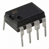
ST7FLITEUS5B6 STMicroelectronics, ST7FLITEUS5B6 Datasheet - Page 35

ST7FLITEUS5B6
Manufacturer Part Number
ST7FLITEUS5B6
Description
MCU 8BIT 1KB FLASH 128KB 8-DIP
Manufacturer
STMicroelectronics
Series
ST7r
Datasheet
1.STEVAL-IFS006V1.pdf
(136 pages)
Specifications of ST7FLITEUS5B6
Core Processor
ST7
Core Size
8-Bit
Speed
8MHz
Peripherals
LVD, POR, PWM, WDT
Number Of I /o
5
Program Memory Size
1KB (1K x 8)
Program Memory Type
FLASH
Ram Size
128 x 8
Voltage - Supply (vcc/vdd)
2.4 V ~ 5.5 V
Data Converters
A/D 5x10b
Oscillator Type
Internal
Operating Temperature
-40°C ~ 85°C
Package / Case
8-DIP (0.300", 7.62mm)
Controller Family/series
ST7
No. Of I/o's
5
Ram Memory Size
128Byte
Cpu Speed
8MHz
No. Of Timers
2
Rohs Compliant
Yes
For Use With
497-6403 - BOARD EVAL 8BIT MICRO + TDE1708497-6407 - BOARD EVAL FOR VACUUM CLEANER497-5861 - EVAL BRD POWER MOSFET/8PIN MCU497-5858 - EVAL BOARD PLAYBACK ST7FLITE497-5515 - EVAL BOARD PHASE CTRL DIMMER497-5049 - KIT STARTER RAISONANCE ST7FLITE497-5046 - KIT TOOL FOR ST7/UPSD/STR7 MCU
Lead Free Status / RoHS Status
Lead free / RoHS Compliant
Eeprom Size
-
Connectivity
-
Other names
497-5636-5
Available stocks
Company
Part Number
Manufacturer
Quantity
Price
Company:
Part Number:
ST7FLITEUS5B6
Manufacturer:
STMicroelectronics
Quantity:
8
ST7LITEUS2, ST7LITEUS5
6.4
6.4.1
Note:
Caution:
Reset sequence manager (RSM)
Introduction
The reset sequence manager includes three reset sources as shown in
●
●
●
A reset can also be triggered following the detection of an illegal opcode or prebyte code.
Refer to
These sources act on the RESET pin and it is always kept low during the delay phase.
The RESET service routine vector is fixed at addresses FFFEh-FFFFh in the ST7 memory
map.
The basic reset sequence consists of 3 phases as shown in
●
●
●
When the ST7 is unprogrammed or fully erased, the Flash is blank and the RESET vector is
not programmed. For this reason, it is recommended to keep the RESET pin in low state
until programming mode is entered, in order to avoid unwanted behavior.
The 64 CPU clock cycle delay allows the oscillator to stabilise and ensures that recovery
has taken place from the Reset state.
The RESET vector fetch phase duration is 2 clock cycles.
Figure 11. Reset sequence phases
External RESET source pulse
Internal LVD reset (low voltage detection)
Internal WATCHDOG reset
Active phase depending on the reset source
64 CPU clock cycle delay
RESET vector fetch
Figure
12.
Active phase
64 CLOCK CYCLES
INTERNAL RESET
RESET
Supply, reset and clock management
VECTOR
FETCH
Figure
11:
Figure
12:
35/136


