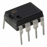
ST7FLITEUS5B6 STMicroelectronics, ST7FLITEUS5B6 Datasheet - Page 59

ST7FLITEUS5B6
Manufacturer Part Number
ST7FLITEUS5B6
Description
MCU 8BIT 1KB FLASH 128KB 8-DIP
Manufacturer
STMicroelectronics
Series
ST7r
Datasheet
1.STEVAL-IFS006V1.pdf
(136 pages)
Specifications of ST7FLITEUS5B6
Core Processor
ST7
Core Size
8-Bit
Speed
8MHz
Peripherals
LVD, POR, PWM, WDT
Number Of I /o
5
Program Memory Size
1KB (1K x 8)
Program Memory Type
FLASH
Ram Size
128 x 8
Voltage - Supply (vcc/vdd)
2.4 V ~ 5.5 V
Data Converters
A/D 5x10b
Oscillator Type
Internal
Operating Temperature
-40°C ~ 85°C
Package / Case
8-DIP (0.300", 7.62mm)
Controller Family/series
ST7
No. Of I/o's
5
Ram Memory Size
128Byte
Cpu Speed
8MHz
No. Of Timers
2
Rohs Compliant
Yes
For Use With
497-6403 - BOARD EVAL 8BIT MICRO + TDE1708497-6407 - BOARD EVAL FOR VACUUM CLEANER497-5861 - EVAL BRD POWER MOSFET/8PIN MCU497-5858 - EVAL BOARD PLAYBACK ST7FLITE497-5515 - EVAL BOARD PHASE CTRL DIMMER497-5049 - KIT STARTER RAISONANCE ST7FLITE497-5046 - KIT TOOL FOR ST7/UPSD/STR7 MCU
Lead Free Status / RoHS Status
Lead free / RoHS Compliant
Eeprom Size
-
Connectivity
-
Other names
497-5636-5
Available stocks
Company
Part Number
Manufacturer
Quantity
Price
Company:
Part Number:
ST7FLITEUS5B6
Manufacturer:
STMicroelectronics
Quantity:
8
ST7LITEUS2, ST7LITEUS5
9
9.1
9.2
9.2.1
Note:
1
2
I/O ports
Introduction
The I/O port offers different functional modes:
●
and for specific pins:
●
●
An I/O port contains up to 6 pins. Each pin (except PA3/RESET) can be programmed
independently as digital input (with or without interrupt generation) or digital output.
Functional description
Each port has 2 main registers:
●
●
and one optional register:
●
Each I/O pin may be programmed using the corresponding register bits in the DDR and OR
registers: bit X corresponding to pin X of the port. The same correspondence is used for the
DR register.
The following description takes into account the OR register, (for specific ports which do not
provide this register refer to the I/O Port Implementation section). The generic I/O block
diagram is shown in
Input modes
The input configuration is selected by clearing the corresponding DDR register bit.
In this case, reading the DR register returns the digital value applied to the external I/O pin.
Different input modes can be selected by software through the OR register.
Writing the DR register modifies the latch value but does not affect the pin status.
PA3 cannot be configured as input.
External interrupt function
When an I/O is configured as Input with Interrupt, an event on this I/O can generate an
external interrupt request to the CPU.
Each pin can independently generate an interrupt request. The interrupt sensitivity is
independently programmable using the sensitivity bits in the EICR register.
External interrupts are hardware interrupts. Fetching the corresponding interrupt vector
automatically clears the request latch. Changing the sensitivity of a particular external
interrupt clears this pending interrupt. This can be used to clear unwanted pending
interrupts.
Transfer of data through digital inputs and outputs
External interrupt generation
Alternate signal input/output for the on-chip peripherals.
Data register (DR)
Data Direction register (DDR)
Option register (OR)
Figure
28.
I/O ports
59/136


