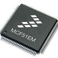
MCF51EM128CLK Freescale Semiconductor, MCF51EM128CLK Datasheet - Page 289

MCF51EM128CLK
Manufacturer Part Number
MCF51EM128CLK
Description
IC MCU 32BIT 128KB FLASH 80LQFP
Manufacturer
Freescale Semiconductor
Series
MCF51EMr
Datasheets
1.MCF51EM128CLL.pdf
(2 pages)
2.MCF51EM128CLL.pdf
(54 pages)
3.MCF51EM128CLL.pdf
(636 pages)
Specifications of MCF51EM128CLK
Core Processor
Coldfire V1
Core Size
32-Bit
Speed
50MHz
Connectivity
I²C, SCI, SPI
Peripherals
LCD, LVD, PWM, WDT
Number Of I /o
56
Program Memory Size
128KB (128K x 8)
Program Memory Type
FLASH
Ram Size
8K x 8
Voltage - Supply (vcc/vdd)
1.8 V ~ 3.6 V
Data Converters
A/D 12x16b
Oscillator Type
External
Operating Temperature
-40°C ~ 85°C
Package / Case
80-LQFP
Processor Series
MCF51EM
Core
ColdFire V1
Data Bus Width
32 bit
Data Ram Size
16 KB
Interface Type
RS-232, LIN
Maximum Clock Frequency
50 MHz
Number Of Timers
3
Operating Supply Voltage
1.8 V to 3.6 V
Maximum Operating Temperature
+ 85 C
Mounting Style
SMD/SMT
3rd Party Development Tools
JLINK-CF-BDM26, EWCF
Development Tools By Supplier
TWR-MCF51CN-KIT, TWR-SER, TWR-ELEV, TOWER
Minimum Operating Temperature
- 40 C
Lead Free Status / RoHS Status
Lead free / RoHS Compliant
Eeprom Size
-
Lead Free Status / Rohs Status
Details
Available stocks
Company
Part Number
Manufacturer
Quantity
Price
Company:
Part Number:
MCF51EM128CLK
Manufacturer:
Freescale Semiconductor
Quantity:
10 000
- Current page: 289 of 636
- Download datasheet (11Mb)
13.1.3
This section includes block diagrams showing SPI system connections, the internal organization of the SPI
module, and the SPI clock dividers that control the master mode bit rate.
13.1.3.1
Figure 13-1
device initiates all SPI data transfers. During a transfer, the master shifts data out (on the MOSI pin) to the
slave while simultaneously shifting data in (on the MISO pin) from the slave. The transfer effectively
exchanges the data that was in the SPI shift registers of the two SPI systems. The SPSCK signal is a clock
output from the master and an input to the slave. The slave device must be selected by a low level on the
slave select input (SS pin). In this system, the master device has configured its SS pin as an optional slave
select output.
13.1.3.2
Figure 13-2
Data is written to the double-buffered transmitter (write to SPIxDH:SPIxDL) and gets transferred to the
SPI shift register at the start of a data transfer. After shifting in 8 or 16 bits (as determined by SPIMODE
bit) of data, the data is transferred into the double-buffered receiver where it can be read (read from
SPIxDH:SPIxDL). Pin multiplexing logic controls connections between MCU pins and the SPI module.
Additionally there is an 8-byte receive FIFO and an 8-byte transmit FIFO that once enabled provide
features to allow less CPU interrupts to occur when transmitting/receiving high volume/high speed data.
When FIFO mode is enabled, the SPI can still function in either 8-bit or 16-bit mode ( as per SPIMODE
bit) and 3 additional flags help monitor the FIFO status and two of these flags can provide CPU interrupts.
When the SPI is configured as a master, the clock output is routed to the SPSCK pin, the shifter output is
routed to MOSI, and the shifter input is routed from the MISO pin.
Freescale Semiconductor
Block Diagrams
is a block diagram of the SPI module. The central element of the SPI is the SPI shift register.
shows the SPI modules of two MCUs connected in a master-slave arrangement. The master
SPI System Block Diagram
SPI Module Block Diagram
GENERATOR
SPI SHIFTER
8 OR 16 BITS
MCF51EM256 Series ColdFire Integrated Microcontroller Reference Manual, Rev. 8
MASTER
CLOCK
Figure 13-1. SPI System Connections
MOSI
MISO
SPSCK
SS
SPSCK
MOSI
MISO
SS
SLAVE
SPI SHIFTER
8 OR 16 BITS
16-Bit Serial Peripheral Interface (SPI16)
13-3
Related parts for MCF51EM128CLK
Image
Part Number
Description
Manufacturer
Datasheet
Request
R

Part Number:
Description:
IC MCU 32BIT 256KB FLASH 100LQFP
Manufacturer:
Freescale Semiconductor
Datasheet:

Part Number:
Description:
BOARD DEMO HARDWARE ONLY
Manufacturer:
Freescale Semiconductor
Datasheet:

Part Number:
Description:
IC MCU 32BIT 128KB FLASH 100LQFP
Manufacturer:
Freescale Semiconductor
Datasheet:

Part Number:
Description:
IC MCU 32BIT 256KB FLASH 80LQFP
Manufacturer:
Freescale Semiconductor
Datasheet:
Part Number:
Description:
Manufacturer:
Freescale Semiconductor, Inc
Datasheet:
Part Number:
Description:
Manufacturer:
Freescale Semiconductor, Inc
Datasheet:
Part Number:
Description:
Manufacturer:
Freescale Semiconductor, Inc
Datasheet:
Part Number:
Description:
Manufacturer:
Freescale Semiconductor, Inc
Datasheet:
Part Number:
Description:
Manufacturer:
Freescale Semiconductor, Inc
Datasheet:
Part Number:
Description:
Manufacturer:
Freescale Semiconductor, Inc
Datasheet:
Part Number:
Description:
Manufacturer:
Freescale Semiconductor, Inc
Datasheet:
Part Number:
Description:
Manufacturer:
Freescale Semiconductor, Inc
Datasheet:
Part Number:
Description:
Manufacturer:
Freescale Semiconductor, Inc
Datasheet:
Part Number:
Description:
Manufacturer:
Freescale Semiconductor, Inc
Datasheet:


