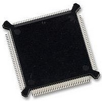
MC68HC16Z1CEH25 Freescale Semiconductor, MC68HC16Z1CEH25 Datasheet - Page 143

MC68HC16Z1CEH25
Manufacturer Part Number
MC68HC16Z1CEH25
Description
IC MCU 16BIT 25MHZ 132-PQFP
Manufacturer
Freescale Semiconductor
Series
HC16r
Datasheet
1.MC68HC16Z1VEH16.pdf
(500 pages)
Specifications of MC68HC16Z1CEH25
Core Processor
CPU16
Core Size
16-Bit
Speed
25MHz
Connectivity
EBI/EMI, SCI, SPI
Peripherals
POR, PWM, WDT
Number Of I /o
16
Program Memory Type
ROMless
Ram Size
1K x 8
Voltage - Supply (vcc/vdd)
2.7 V ~ 5.5 V
Data Converters
A/D 8x10b
Oscillator Type
Internal
Operating Temperature
-40°C ~ 85°C
Package / Case
132-QFP
Package
132PQFP
Family Name
HC16
Maximum Speed
25 MHz
Operating Supply Voltage
3.3|5 V
Data Bus Width
16 Bit
Number Of Programmable I/os
16
On-chip Adc
8-chx10-bit
Number Of Timers
11
Controller Family/series
68HC16
No. Of I/o's
16
Ram Memory Size
1KB
Cpu Speed
25MHz
No. Of Timers
2
Embedded Interface Type
QSPI, SCI
Rohs Compliant
Yes
Processor Series
HC16Z
Core
CPU16
Data Ram Size
1 KB
Interface Type
SCI, SPI, UART
Maximum Clock Frequency
25 MHz
Maximum Operating Temperature
+ 85 C
Mounting Style
SMD/SMT
Minimum Operating Temperature
- 40 C
Lead Free Status / RoHS Status
Lead free / RoHS Compliant
Eeprom Size
-
Program Memory Size
-
Lead Free Status / Rohs Status
Details
Available stocks
Company
Part Number
Manufacturer
Quantity
Price
Company:
Part Number:
MC68HC16Z1CEH25
Manufacturer:
Freescale Semiconductor
Quantity:
135
Company:
Part Number:
MC68HC16Z1CEH25
Manufacturer:
Freescale Semiconductor
Quantity:
10 000
- Current page: 143 of 500
- Download datasheet (6Mb)
5.6.2 Regular Bus Cycle
5.6.2.1 Read Cycle
M68HC16 Z SERIES
USER’S MANUAL
Descriptions are made in terms of individual system clock states, labelled {S0, S1,
S2,..., SN}. The designation “state” refers to the logic level of the clock signal, and
does not correspond to any implemented machine state. A clock cycle consists of two
successive states. Refer to
more information on clock control timing.
Bus cycles terminated by DSACK assertion normally require a minimum of three
CLKOUT cycles. To support systems that use CLKOUT to generate DSACK and other
inputs, asynchronous input setup time and asynchronous input hold times are speci-
fied. When these specifications are met, the MCU is guaranteed to recognize the ap-
propriate signal on a specific edge of the CLKOUT signal.
The following paragraphs contain a discussion of cycles that use external bus control
logic. Refer to
cycles.
To initiate a transfer, the MCU asserts an address and the SIZ[1:0] signals. The SIZ
signals and ADDR0 are externally decoded to select the active portion of the data bus.
Refer to
device either places data on the bus (read cycle) or latches data from the bus (write
cycle), then asserts a DSACK[1:0] combination that indicates port size.
The DSACK[1:0] signals can be asserted before the data from a peripheral device is
valid on a read cycle. To ensure valid data is latched into the MCU, a maximum period
between DSACK assertion and DS assertion is specified.
There is no specified maximum for the period between the assertion of AS and
DSACK. Although the MCU can transfer data in a minimum of three clock cycles when
the cycle is terminated with DSACK, the MCU inserts wait cycles in clock period incre-
ments until either DSACK signal goes low.
If bus termination signals remain unasserted, the MCU will continue to insert wait
states, and the bus cycle will never end. If no peripheral responds to an access, or if
an access is invalid, external logic should assert the BERR or HALT signals to abort
the bus cycle (when BERR and HALT are asserted simultaneously, the CPU16 acts
as though only BERR is asserted). When enabled, the SIM bus monitor asserts BERR
when DSACK response time exceeds a predetermined limit. The bus monitor time-out
period is determined by the BMT[1:0] field in SYPCR. The maximum bus monitor time-
out period is 64 system clock cycles.
During a read cycle, the MCU transfers data from an external memory or peripheral
device. If the instruction specifies a long-word or word operation, the MCU attempts to
read two bytes at once. For a byte operation, the MCU reads one byte. The portion of
the data bus from which each byte is read depends on operand size, peripheral ad-
dress, and peripheral port size.
to
Manual (SIMRM/AD) for more information.
5.5.2 Dynamic Bus
5.5.2 Dynamic Bus
5.6.3 Fast Termination Cycles
Freescale Semiconductor, Inc.
For More Information On This Product,
Sizing,
SYSTEM INTEGRATION MODULE
APPENDIX A ELECTRICAL CHARACTERISTICS
Go to: www.freescale.com
Sizing. When AS, DS, and R/W are valid, a peripheral
5.5.4 Misaligned
Figure 5-12
is a flowchart of a word read cycle. Refer
for information about fast termination
Operands, and the SIM Reference
5-37
for
Related parts for MC68HC16Z1CEH25
Image
Part Number
Description
Manufacturer
Datasheet
Request
R
Part Number:
Description:
Manufacturer:
Freescale Semiconductor, Inc
Datasheet:
Part Number:
Description:
Manufacturer:
Freescale Semiconductor, Inc
Datasheet:
Part Number:
Description:
Manufacturer:
Freescale Semiconductor, Inc
Datasheet:
Part Number:
Description:
Manufacturer:
Freescale Semiconductor, Inc
Datasheet:
Part Number:
Description:
Manufacturer:
Freescale Semiconductor, Inc
Datasheet:
Part Number:
Description:
Manufacturer:
Freescale Semiconductor, Inc
Datasheet:
Part Number:
Description:
Manufacturer:
Freescale Semiconductor, Inc
Datasheet:
Part Number:
Description:
Manufacturer:
Freescale Semiconductor, Inc
Datasheet:
Part Number:
Description:
Manufacturer:
Freescale Semiconductor, Inc
Datasheet:
Part Number:
Description:
Manufacturer:
Freescale Semiconductor, Inc
Datasheet:
Part Number:
Description:
Manufacturer:
Freescale Semiconductor, Inc
Datasheet:
Part Number:
Description:
Manufacturer:
Freescale Semiconductor, Inc
Datasheet:
Part Number:
Description:
Manufacturer:
Freescale Semiconductor, Inc
Datasheet:
Part Number:
Description:
Manufacturer:
Freescale Semiconductor, Inc
Datasheet:
Part Number:
Description:
Manufacturer:
Freescale Semiconductor, Inc
Datasheet:


