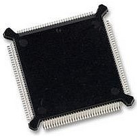
MC68HC16Z1CEH25 Freescale Semiconductor, MC68HC16Z1CEH25 Datasheet - Page 160

MC68HC16Z1CEH25
Manufacturer Part Number
MC68HC16Z1CEH25
Description
IC MCU 16BIT 25MHZ 132-PQFP
Manufacturer
Freescale Semiconductor
Series
HC16r
Datasheet
1.MC68HC16Z1VEH16.pdf
(500 pages)
Specifications of MC68HC16Z1CEH25
Core Processor
CPU16
Core Size
16-Bit
Speed
25MHz
Connectivity
EBI/EMI, SCI, SPI
Peripherals
POR, PWM, WDT
Number Of I /o
16
Program Memory Type
ROMless
Ram Size
1K x 8
Voltage - Supply (vcc/vdd)
2.7 V ~ 5.5 V
Data Converters
A/D 8x10b
Oscillator Type
Internal
Operating Temperature
-40°C ~ 85°C
Package / Case
132-QFP
Package
132PQFP
Family Name
HC16
Maximum Speed
25 MHz
Operating Supply Voltage
3.3|5 V
Data Bus Width
16 Bit
Number Of Programmable I/os
16
On-chip Adc
8-chx10-bit
Number Of Timers
11
Controller Family/series
68HC16
No. Of I/o's
16
Ram Memory Size
1KB
Cpu Speed
25MHz
No. Of Timers
2
Embedded Interface Type
QSPI, SCI
Rohs Compliant
Yes
Processor Series
HC16Z
Core
CPU16
Data Ram Size
1 KB
Interface Type
SCI, SPI, UART
Maximum Clock Frequency
25 MHz
Maximum Operating Temperature
+ 85 C
Mounting Style
SMD/SMT
Minimum Operating Temperature
- 40 C
Lead Free Status / RoHS Status
Lead free / RoHS Compliant
Eeprom Size
-
Program Memory Size
-
Lead Free Status / Rohs Status
Details
Available stocks
Company
Part Number
Manufacturer
Quantity
Price
Company:
Part Number:
MC68HC16Z1CEH25
Manufacturer:
Freescale Semiconductor
Quantity:
135
Company:
Part Number:
MC68HC16Z1CEH25
Manufacturer:
Freescale Semiconductor
Quantity:
10 000
- Current page: 160 of 500
- Download datasheet (6Mb)
5.7.5.1 Reset States of SIM Pins
5.7.5.2 Reset States of Pins Assigned to Other MCU Modules
5-54
Generally, while RESET is asserted, SIM pins either go to an inactive high-impedance
state or are driven to their inactive states. After RESET is released, mode selection
occurs, and reset exception processing begins. Pins configured as inputs must be
driven to the desired active state. Pull-up or pull-down circuitry may be necessary. Pins
configured as outputs begin to function after RESET is released.
mary of SIM pin states during reset.
As a rule, module pins that are assigned to general-purpose I/O ports go into a high-
impedance state following reset. However, during power-on reset, module port pins
may be in an indeterminate state for a short period. Refer to
for more information.
CS[9:6]/ADDR[22:19]/PC[6:3]
CS[5:3]/FC[2:0]/PC[2:0]
CS10/ADDR23/ECLK
IRQ[7:1]/PF[7:1]
SIZ[1:0]/PE[7:6]
MODCLK/PF0
DSACK0/PE0
DSACK1/PE1
CS2/BGACK
ADDR[18:0]
DATA[15:0]
AVEC/PE2
CSBOOT
CLKOUT
CS1/BG
CS0/BR
AS/PE5
DS/PE4
RESET
Pin(s)
BERR
HALT
R/W
TSC
Pins that are not used should either be configured as outputs, or (if
configured as inputs) pulled to the appropriate inactive state. This de-
creases additional I
ply level.
Freescale Semiconductor, Inc.
For More Information On This Product,
Table 5-21 SIM Pin Reset States
While RESET
Mode Select
Mode select
Mode select
SYSTEM INTEGRATION MODULE
Pin State
Asserted
Asserted
High-Z
High-Z
High-Z
High-Z
Output
High-Z
High-Z
High-Z
High-Z
High-Z
High-Z
High-Z
V
V
V
V
V
V
V
DD
DD
DD
DD
DD
DD
DD
Go to: www.freescale.com
DD
caused by digital inputs floating near mid-sup-
Pin Function
ADDR[18:0]
DATA[15:0]
CSBOOT
MODCLK
CLKOUT
DSACK0
DSACK1
IRQ[7:1]
SIZ[1:0]
CS[9:6]
CS[5:3]
RESET
AVEC
BERR
HALT
CS10
TSC
CS1
CS2
CS0
R/W
Default Function
AS
DS
NOTE
Pin State After RESET Released
Pin State
Unknown
Unknown
Output
Output
Output
Output
Input
Input
Input
Input
Input
Input
Input
Input
Input
Input
V
V
V
V
V
V
V
DD
DD
DD
DD
DD
SS
DD
Pin Function
ADDR[22:19]
ADDR[18:0]
DATA[15:0]
CSBOOT
CLKOUT
ADDR23
5.7.7 Power-On Reset
BGACK
RESET
FC[2:0]
PF[7:1]
PE[7:6]
BERR
HALT
Alternate Function
R/W
TSC
PE5
PE2
PE4
PE0
PE1
PF0
BG
BR
Table 5-21
M68HC16 Z SERIES
USER’S MANUAL
Pin State
Unknown
Unknown
Unknown
Unknown
Output
Output
Input
Input
Input
Input
Input
Input
Input
Input
Input
Input
Input
Input
Input
Input
Input
V
V
is a sum-
DD
SS
Related parts for MC68HC16Z1CEH25
Image
Part Number
Description
Manufacturer
Datasheet
Request
R
Part Number:
Description:
Manufacturer:
Freescale Semiconductor, Inc
Datasheet:
Part Number:
Description:
Manufacturer:
Freescale Semiconductor, Inc
Datasheet:
Part Number:
Description:
Manufacturer:
Freescale Semiconductor, Inc
Datasheet:
Part Number:
Description:
Manufacturer:
Freescale Semiconductor, Inc
Datasheet:
Part Number:
Description:
Manufacturer:
Freescale Semiconductor, Inc
Datasheet:
Part Number:
Description:
Manufacturer:
Freescale Semiconductor, Inc
Datasheet:
Part Number:
Description:
Manufacturer:
Freescale Semiconductor, Inc
Datasheet:
Part Number:
Description:
Manufacturer:
Freescale Semiconductor, Inc
Datasheet:
Part Number:
Description:
Manufacturer:
Freescale Semiconductor, Inc
Datasheet:
Part Number:
Description:
Manufacturer:
Freescale Semiconductor, Inc
Datasheet:
Part Number:
Description:
Manufacturer:
Freescale Semiconductor, Inc
Datasheet:
Part Number:
Description:
Manufacturer:
Freescale Semiconductor, Inc
Datasheet:
Part Number:
Description:
Manufacturer:
Freescale Semiconductor, Inc
Datasheet:
Part Number:
Description:
Manufacturer:
Freescale Semiconductor, Inc
Datasheet:
Part Number:
Description:
Manufacturer:
Freescale Semiconductor, Inc
Datasheet:


