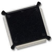
MC68HC16Z1CEH25 Freescale Semiconductor, MC68HC16Z1CEH25 Datasheet - Page 249

MC68HC16Z1CEH25
Manufacturer Part Number
MC68HC16Z1CEH25
Description
IC MCU 16BIT 25MHZ 132-PQFP
Manufacturer
Freescale Semiconductor
Series
HC16r
Datasheet
1.MC68HC16Z1VEH16.pdf
(500 pages)
Specifications of MC68HC16Z1CEH25
Core Processor
CPU16
Core Size
16-Bit
Speed
25MHz
Connectivity
EBI/EMI, SCI, SPI
Peripherals
POR, PWM, WDT
Number Of I /o
16
Program Memory Type
ROMless
Ram Size
1K x 8
Voltage - Supply (vcc/vdd)
2.7 V ~ 5.5 V
Data Converters
A/D 8x10b
Oscillator Type
Internal
Operating Temperature
-40°C ~ 85°C
Package / Case
132-QFP
Package
132PQFP
Family Name
HC16
Maximum Speed
25 MHz
Operating Supply Voltage
3.3|5 V
Data Bus Width
16 Bit
Number Of Programmable I/os
16
On-chip Adc
8-chx10-bit
Number Of Timers
11
Controller Family/series
68HC16
No. Of I/o's
16
Ram Memory Size
1KB
Cpu Speed
25MHz
No. Of Timers
2
Embedded Interface Type
QSPI, SCI
Rohs Compliant
Yes
Processor Series
HC16Z
Core
CPU16
Data Ram Size
1 KB
Interface Type
SCI, SPI, UART
Maximum Clock Frequency
25 MHz
Maximum Operating Temperature
+ 85 C
Mounting Style
SMD/SMT
Minimum Operating Temperature
- 40 C
Lead Free Status / RoHS Status
Lead free / RoHS Compliant
Eeprom Size
-
Program Memory Size
-
Lead Free Status / Rohs Status
Details
Available stocks
Company
Part Number
Manufacturer
Quantity
Price
Company:
Part Number:
MC68HC16Z1CEH25
Manufacturer:
Freescale Semiconductor
Quantity:
135
Company:
Part Number:
MC68HC16Z1CEH25
Manufacturer:
Freescale Semiconductor
Quantity:
10 000
- Current page: 249 of 500
- Download datasheet (6Mb)
10.3.4.1 CPHA = 0 Transfer Format
M68HC16 Z SERIES
USER’S MANUAL
SCK (CPOL = 0)
SCK (CPOL = 1)
(FROM MASTER)
(FROM SLAVE)
SS (TO SLAVE)
MISO
Figure 10-3
equals zero. Two waveforms are shown for SCK: one for CPOL equal to zero and an-
other for CPOL equal to one. The diagram may be interpreted as a master or slave
timing diagram since the SCK, MISO and MOSI pins are directly connected between
the master and the slave. The MISO signal shown is the output from the slave and the
MOSI signal shown is the output from the master. The SS line is the chip-select input
to the slave.
For a master, writing to the SPDR initiates the transfer. For a slave, the falling edge of
SS indicates the start of a transfer. The SCK signal remains inactive for the first half
of the first SCK cycle. Data is latched on the first and each succeeding odd clock edge,
and the SPI shift register is left-shifted on the second and succeeding even clock edg-
es. SPIF is set at the end of the eighth SCK cycle.
When CPHA equals zero, the SS line must be negated and reasserted between each
successive serial byte. If the slave writes data to the SPI data register while SS is as-
serted (low), a write collision error results. To avoid this problem, the slave should read
bit three of PORTMCP, which indicates the state of the SS pin, before writing to the
SPDR again.
MOSI
(FOR REFERENCE)
SCK CYCLE #
is a timing diagram of an 8-bit, MSB-first SPI transfer in which CPHA
Figure 10-3 CPHA = 0 SPI Transfer Format
MSB
MULTICHANNEL COMMUNICATION INTERFACE
Freescale Semiconductor, Inc.
MSB
1
For More Information On This Product,
2
6
6
Go to: www.freescale.com
3
5
5
4
4
4
5
3
3
6
2
2
7
1
1
LSB
LSB
8
CPHA = 0 SPI TRANSFER
10-9
Related parts for MC68HC16Z1CEH25
Image
Part Number
Description
Manufacturer
Datasheet
Request
R
Part Number:
Description:
Manufacturer:
Freescale Semiconductor, Inc
Datasheet:
Part Number:
Description:
Manufacturer:
Freescale Semiconductor, Inc
Datasheet:
Part Number:
Description:
Manufacturer:
Freescale Semiconductor, Inc
Datasheet:
Part Number:
Description:
Manufacturer:
Freescale Semiconductor, Inc
Datasheet:
Part Number:
Description:
Manufacturer:
Freescale Semiconductor, Inc
Datasheet:
Part Number:
Description:
Manufacturer:
Freescale Semiconductor, Inc
Datasheet:
Part Number:
Description:
Manufacturer:
Freescale Semiconductor, Inc
Datasheet:
Part Number:
Description:
Manufacturer:
Freescale Semiconductor, Inc
Datasheet:
Part Number:
Description:
Manufacturer:
Freescale Semiconductor, Inc
Datasheet:
Part Number:
Description:
Manufacturer:
Freescale Semiconductor, Inc
Datasheet:
Part Number:
Description:
Manufacturer:
Freescale Semiconductor, Inc
Datasheet:
Part Number:
Description:
Manufacturer:
Freescale Semiconductor, Inc
Datasheet:
Part Number:
Description:
Manufacturer:
Freescale Semiconductor, Inc
Datasheet:
Part Number:
Description:
Manufacturer:
Freescale Semiconductor, Inc
Datasheet:
Part Number:
Description:
Manufacturer:
Freescale Semiconductor, Inc
Datasheet:


