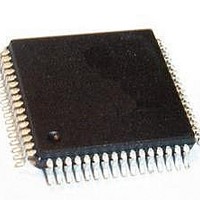
SAK-XC888CLM-8FFA 5V AC Infineon Technologies, SAK-XC888CLM-8FFA 5V AC Datasheet - Page 59

SAK-XC888CLM-8FFA 5V AC
Manufacturer Part Number
SAK-XC888CLM-8FFA 5V AC
Description
IC MCU 8BIT FLASH 64-LQFP
Manufacturer
Infineon Technologies
Series
XC8xxr
Datasheet
1.SAF-XC888CLM-6FFA_5V_AC.pdf
(144 pages)
Specifications of SAK-XC888CLM-8FFA 5V AC
Core Processor
XC800
Core Size
8-Bit
Speed
103.2MHz
Connectivity
CAN, LIN, SSI, UART/USART
Peripherals
Brown-out Detect/Reset, POR, PWM, WDT
Number Of I /o
48
Program Memory Size
32KB (32K x 8)
Program Memory Type
FLASH
Ram Size
1.75K x 8
Voltage - Supply (vcc/vdd)
4.5 V ~ 5.5 V
Data Converters
A/D 8x10b
Oscillator Type
Internal
Operating Temperature
-40°C ~ 125°C
Package / Case
64-LFQFP
Data Bus Width
8 bit
Data Ram Size
1.75 KB
Interface Type
UART, SSC
Maximum Clock Frequency
24 MHz
Number Of Programmable I/os
48
Number Of Timers
4
Operating Supply Voltage
5 V
Maximum Operating Temperature
+ 125 C
Mounting Style
SMD/SMT
Minimum Operating Temperature
- 40 C
On-chip Adc
10 bit, 8 Channel
For Use With
B158-H8743-X-X-7600IN - KIT STARTER XC886/888
Lead Free Status / RoHS Status
Lead free / RoHS Compliant
Eeprom Size
-
Lead Free Status / Rohs Status
Details
Other names
SP000210982
- Current page: 59 of 144
- Download datasheet (2Mb)
3.3
The Flash memory provides an embedded user-programmable non-volatile memory,
allowing fast and reliable storage of user code and data. It is operated from a single 2.5 V
supply from the Embedded Voltage Regulator (EVR) and does not require additional
programming or erasing voltage. The sectorization of the Flash memory allows each
sector to be erased independently.
Features
•
•
•
•
•
•
•
•
•
•
•
•
•
1) P-Flash: 64-byte wordline can only be programmed once, i.e., one gate disturb allowed.
2) Values shown here are typical values.
3) Values shown here are typical values.
Data Sheet
D-Flash: 32-byte wordline can be programmed twice, i.e., two gate disturbs allowed.
frequency range for Flash read access.
programming and erasing.
In-System Programming (ISP) via UART
In-Application Programming (IAP)
Error Correction Code (ECC) for dynamic correction of single-bit errors
Background program and erase operations for CPU load minimization
Support for aborting erase operation
Minimum program width
1-sector minimum erase width
1-byte read access
Flash is delivered in erased state (read all zeros)
Operating supply voltage: 2.5 V ± 7.5 %
Read access time: 3 ×
Program time: 248256 /
Erase time: 9807360 /
Flash Memory
f
sysmin
f
t
SYS
CCLK
1)
f
SYS
is used for obtaining the worst case timing.
of 32-byte for D-Flash and 64-byte for P-Flash
= 102 ms
= 125 ns
= 2.6 ms
f
sys
f
sys
= 96 MHz ± 7.5% (
= 96 MHz ± 7.5% is the only frequency range for Flash
3)
2)
3)
52
f
CCLK
= 24 MHz ± 7.5 %) is the maximum
Functional Description
XC886/888CLM
V1.2, 2009-07
Related parts for SAK-XC888CLM-8FFA 5V AC
Image
Part Number
Description
Manufacturer
Datasheet
Request
R

Part Number:
Description:
IC MCU 8BIT FLASH 64-LQFP
Manufacturer:
Infineon Technologies
Datasheet:

Part Number:
Description:
IC MCU 8BIT FLASH 64-TQFP
Manufacturer:
Infineon Technologies
Datasheet:

Part Number:
Description:
High Performance 8-bit Microcontroller With On-chip Flash Memory And Can
Manufacturer:
Infineon Technologies Corporation
Datasheet:

Part Number:
Description:
IC MCU 8BIT FLASH TQFP-64
Manufacturer:
Infineon Technologies
Datasheet:

Part Number:
Description:
IC MCU 8BIT FLASH 64-LQFP
Manufacturer:
Infineon Technologies
Datasheet:

Part Number:
Description:
IC MCU 8BIT FLASH 64-LQFP
Manufacturer:
Infineon Technologies
Datasheet:

Part Number:
Description:
IC MCU 8BIT FLASH 64-LQFP
Manufacturer:
Infineon Technologies
Datasheet:

Part Number:
Description:
Manufacturer:
Infineon Technologies AG
Datasheet:

Part Number:
Description:
Manufacturer:
Infineon Technologies AG
Datasheet:

Part Number:
Description:
Manufacturer:
Infineon Technologies AG
Datasheet:

Part Number:
Description:
Manufacturer:
Infineon Technologies AG
Datasheet:

Part Number:
Description:
Manufacturer:
Infineon Technologies AG
Datasheet:

Part Number:
Description:
Manufacturer:
Infineon Technologies AG
Datasheet:

Part Number:
Description:
Manufacturer:
Infineon Technologies AG
Datasheet:

Part Number:
Description:
16-bit microcontroller with 2x2 KByte RAM
Manufacturer:
Infineon Technologies AG
Datasheet:


