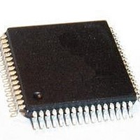
SAK-XC888CLM-8FFA 5V AC Infineon Technologies, SAK-XC888CLM-8FFA 5V AC Datasheet - Page 60

SAK-XC888CLM-8FFA 5V AC
Manufacturer Part Number
SAK-XC888CLM-8FFA 5V AC
Description
IC MCU 8BIT FLASH 64-LQFP
Manufacturer
Infineon Technologies
Series
XC8xxr
Datasheet
1.SAF-XC888CLM-6FFA_5V_AC.pdf
(144 pages)
Specifications of SAK-XC888CLM-8FFA 5V AC
Core Processor
XC800
Core Size
8-Bit
Speed
103.2MHz
Connectivity
CAN, LIN, SSI, UART/USART
Peripherals
Brown-out Detect/Reset, POR, PWM, WDT
Number Of I /o
48
Program Memory Size
32KB (32K x 8)
Program Memory Type
FLASH
Ram Size
1.75K x 8
Voltage - Supply (vcc/vdd)
4.5 V ~ 5.5 V
Data Converters
A/D 8x10b
Oscillator Type
Internal
Operating Temperature
-40°C ~ 125°C
Package / Case
64-LFQFP
Data Bus Width
8 bit
Data Ram Size
1.75 KB
Interface Type
UART, SSC
Maximum Clock Frequency
24 MHz
Number Of Programmable I/os
48
Number Of Timers
4
Operating Supply Voltage
5 V
Maximum Operating Temperature
+ 125 C
Mounting Style
SMD/SMT
Minimum Operating Temperature
- 40 C
On-chip Adc
10 bit, 8 Channel
For Use With
B158-H8743-X-X-7600IN - KIT STARTER XC886/888
Lead Free Status / RoHS Status
Lead free / RoHS Compliant
Eeprom Size
-
Lead Free Status / Rohs Status
Details
Other names
SP000210982
Table 19
Table 19
Retention
Program Flash
20 years
20 years
Data Flash
20 years
5 years
2 years
2 years
1) One cycle refers to the programming of all wordlines in a sector and erasing of sector. The Flash endurance
2) If no Flash is used for data, the Program Flash size can be up to the maximum Flash size available in the
3.3.1
The XC886/888 product family offers Flash devices with either 24 Kbytes or 32 Kbytes
of embedded Flash memory. Each Flash device consists of Program Flash (P-Flash)
and Data Flash (D-Flash) bank(s) with different sectorization shown in
types can be used for code and data storage. The label “Data” neither implies that the
D-Flash is mapped to the data memory region, nor that it can only be used for data
storage. It is used to distinguish the different Flash bank sectorizations.
The 32-Kbyte Flash device consists of 6 P-Flash and 2 D-Flash banks, while the 24-
Kbyte Flash device consists of also of 6 P-Flash banks but with the upper 2 banks only
2 Kbytes each, and only 1 D-Flash bank. The XC886/888 ROM devices offer a single 4-
Kbyte D-Flash bank.
The P-Flash banks are always grouped in pairs. As such, the P-Flash banks are also
sometimes referred to as P-Flash bank pair. Each sector in a P-Flash bank is grouped
with the corresponding sector from the other bank within a bank pair to form a P-Flash
bank pair sector.
Data Sheet
data specified in
- the maximum number of erase cycles per Flash sector must not exceed 100,000 cycles.
- the maximum number of erase cycles per Flash bank must not exceed 300,000 cycles.
- the maximum number of program cycles per Flash bank must not exceed 2,500,000 cycles.
device variant. Having more Data Flash will mean less Flash is available for Program Flash.
shows the Flash data retention and endurance targets.
Flash Bank Sectorization
Flash Data Retention and Endurance (Operating Conditions apply)
Table 19
Endurance
1,000 cycles
1,000 cycles
1,000 cycles
10,000 cycles
70,000 cycles
100,000 cycles
is valid only if the following conditions are fulfilled:
1)
53
4 Kbytes
Size
up to 32 Kbytes
up to 24 Kbytes
1 Kbyte
512 bytes
128 bytes
2)
2)
Functional Description
Remarks
for 32-Kbyte Variant
for 24-Kbyte Variant
XC886/888CLM
Figure
V1.2, 2009-07
11. Both


