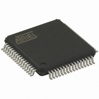
AT89C5122D-RDRIM Atmel, AT89C5122D-RDRIM Datasheet - Page 102

AT89C5122D-RDRIM
Manufacturer Part Number
AT89C5122D-RDRIM
Description
IC MCU 80C51 W/SMART CARD 64VQFP
Manufacturer
Atmel
Series
89Cr
Specifications of AT89C5122D-RDRIM
Core Processor
8051
Core Size
8-Bit
Speed
48MHz
Connectivity
SmartCard, SPI, UART/USART, USB
Peripherals
LED, POR, WDT
Number Of I /o
46
Program Memory Size
32KB (32K x 8)
Program Memory Type
FLASH
Ram Size
768 x 8
Voltage - Supply (vcc/vdd)
3 V ~ 5.5 V
Oscillator Type
Internal
Operating Temperature
-40°C ~ 85°C
Package / Case
64-TQFP, 64-VQFP
For Use With
AT89STK-10 - KIT EVAL APPL MASS STORAGEAT89STK-03 - KIT STARTER FOR MCU AT8XC5122/23
Lead Free Status / RoHS Status
Contains lead / RoHS non-compliant
Eeprom Size
-
Data Converters
-
Other names
AT89C5122DRDRIMTR
Available stocks
Company
Part Number
Manufacturer
Quantity
Price
- Current page: 102 of 208
- Download datasheet (3Mb)
Bulk/Interrupt OUT
Transactions in Ping-Pong
Mode (Endpoints 6)
102
AT83R5122, AT8xC5122/23
Figure 55. Bulk / Interrupt OUT Transactions in Ping-Pong Mode
An endpoint should be first enabled and configured before being able to receive Bulk or
Interrupt packets.
When a valid OUT packet is received on the endpoint bank 0, the RXOUTB0 bit is set by
the USB controller. This triggers an interrupt if enabled. The firmware has to select the
corresponding endpoint, store the number of data bytes by reading the UBYCTX regis-
ter. If the received packet is a ZLP (Zero Length Packet), the UBYCTX register value is
equal to 0 and no data has to be read.
When all the endpoint FIFO bytes have been read, the firmware should clear the
RXOUB0 bit to allow the USB controller to accept the next OUT packet on the endpoint
bank 0. This action switches the endpoint bank 0 and 1. Until the RXOUTB0 bit has
been cleared by the firmware, the USB controller will answer a NAK handshake for each
OUT requests on the bank 0 endpoint FIFO.
When a new valid OUT packet is received on the endpoint bank 1, the RXOUTB1 bit is
set by the USB controller. This triggers an interrupt if enabled. The firmware empties the
bank 1 endpoint FIFO before clearing the RXOUTB1 bit. Until the RXOUTB1 bit has
been cleared by the firmware, the USB controller will answer a NAK handshake for each
OUT requests on the bank 1 endpoint FIFO.
The RXOUTB0 and RXOUTB1 bits are alternatively set by the USB controller at each
new valid packet receipt.
The firmware has to clear one of these two bits after having read all the data FIFO to
allow a new valid packet to be stored in the corresponding bank.
A NAK handshake is sent by the USB controller only if the banks 0 and 1 has not been
released by the firmware.
OUT
OUT
OUT
HOST
DATA0 (n bytes)
DATA1 (m bytes)
DATA0 (p bytes)
ACK
ACK
ACK
UFI
RXOUTB0
RXOUTB1
RXOUTB0
Endpoint FIFO bank 0 - read byte 1
Endpoint FIFO bank 0 - read byte 2
Endpoint FIFO bank 0 - read byte n
Endpoint FIFO bank 1 - read byte 1
Endpoint FIFO bank 1 - read byte 2
Endpoint FIFO bank 1 - read byte m
Endpoint FIFO bank 0 - read byte 1
Endpoint FIFO bank 0 - read byte 2
Endpoint FIFO bank 0 - read byte p
Clear RXOUTB0
Clear RXOUTB1
Clear RXOUTB0
C51
4202F–SCR–07/2008
Related parts for AT89C5122D-RDRIM
Image
Part Number
Description
Manufacturer
Datasheet
Request
R

Part Number:
Description:
IC 8051 MCU 32K CRAM USB 64-VQFP
Manufacturer:
Atmel
Datasheet:

Part Number:
Description:
IC 8051 MCU W/SMART CARD 64VQFP
Manufacturer:
Atmel
Datasheet:

Part Number:
Description:
IC 8051 MCU FLASH 32K 64QFN
Manufacturer:
Atmel
Datasheet:

Part Number:
Description:
IC 8051 MCU FLASH 32K 64VQFP
Manufacturer:
Atmel
Datasheet:

Part Number:
Description:
IC 8051 MCU FLASH 32K 28PLCC
Manufacturer:
Atmel
Datasheet:

Part Number:
Description:
MICROCONTROLLER WITH USB AND SMART CARD READER INTERFACES
Manufacturer:
ATMEL [ATMEL Corporation]
Datasheet:

Part Number:
Description:
KIT STARTER FOR MCU AT8XC5122/23
Manufacturer:
Atmel
Datasheet:

Part Number:
Description:
IC MICRO CTRL 24MHZ 44TQFP
Manufacturer:
Atmel
Datasheet:

Part Number:
Description:
IC MICRO CTRL 24MHZ 44PLCC
Manufacturer:
Atmel
Datasheet:

Part Number:
Description:
IC MICRO CTRL 24MHZ 44PLCC
Manufacturer:
Atmel
Datasheet:

Part Number:
Description:
IC MICRO CTRL 24MHZ 40DIP
Manufacturer:
Atmel
Datasheet:


