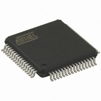
AT89C5122D-RDRIM Atmel, AT89C5122D-RDRIM Datasheet - Page 184

AT89C5122D-RDRIM
Manufacturer Part Number
AT89C5122D-RDRIM
Description
IC MCU 80C51 W/SMART CARD 64VQFP
Manufacturer
Atmel
Series
89Cr
Specifications of AT89C5122D-RDRIM
Core Processor
8051
Core Size
8-Bit
Speed
48MHz
Connectivity
SmartCard, SPI, UART/USART, USB
Peripherals
LED, POR, WDT
Number Of I /o
46
Program Memory Size
32KB (32K x 8)
Program Memory Type
FLASH
Ram Size
768 x 8
Voltage - Supply (vcc/vdd)
3 V ~ 5.5 V
Oscillator Type
Internal
Operating Temperature
-40°C ~ 85°C
Package / Case
64-TQFP, 64-VQFP
For Use With
AT89STK-10 - KIT EVAL APPL MASS STORAGEAT89STK-03 - KIT STARTER FOR MCU AT8XC5122/23
Lead Free Status / RoHS Status
Contains lead / RoHS non-compliant
Eeprom Size
-
Data Converters
-
Other names
AT89C5122DRDRIMTR
Available stocks
Company
Part Number
Manufacturer
Quantity
Price
- Current page: 184 of 208
- Download datasheet (3Mb)
Electrical Characteristics
Absolute Maximum Ratings
DC Parameters
T
184
Symbol
V
V
V
V
V
V
V
I
I
I
R
R
CIO
DV
DI
V
V
t
IL
LI
TL
rise,
Ambiant Temperature Under Bias ......................-25 C to 85 C
Storage Temperature .................................... -65 C to + 150 C
Voltage on V
Voltage on Any Pin to V
Power Dissipation 1 W
A
IL
IH
IH1
OL
OH
OL1
OH1
PFDP
PFDM
MEDIUM
WEAK
CC
= -40 to +85 C; V
CC
t
fall
AT83R5122, AT8xC5122/23
Parameter
Input Low Voltage
Input High Voltage except XTAL1, RST
Input High Voltage, XTAL1, RST
Output Low Voltage: P0, ALE, PSEN
Output High Voltage: P0, ALE, PSEN
Output Low Voltage: P2, P3, P4, P5, P1.2, P1.6,
P1.7
Output High Voltage: P2, P3, P4, P5, P1.2, P1.6,
P1.7
Logical 0 Input Current ports 2 to 5 and P1.2, P1.6,
P1.7, if Weak pull-up enabled
Input Leakage Current
Logical 1 to O transistion Current, Port 51
configuration
Medium Pullup Resistor
Weak Pullup Resistor
Capacitance of I/O Buffer
Digital Supply Voltage
Digital Supply Output Current (DVcc pin)
Power Fail High Level Threshold
Power Fail Low Level Threshold
V
DD
CC
rise and fall time
to V
SS
SS
......................................-0.5 V to + 6.0V
SS
= 0 V, F
........................-0.5 V to V
CK_CPU
= 0 to 24 MHz , V
CC
+ 0.5 V
0.2 V
CC
0.7 V
0.9 V
0.9 V
Min
-0.5
1 s
= 3.0V to 5.5V
CC
2,5
3
CC
CC
CC
+ 0.9
Note:
Typ
100
3.4
2.8
2.6
10
Stresses at or above those listed under “Absolute
Maximum Ratings” may cause permanent damage to
the device. This is a stress rating only and functional
operation of the device at these or any other condi-
tions above those indicated in the operational
sections of this specification is not implied. Exposure
to absolute maximum rating conditions may affect
device reliability.
Power Dissipation value is based on the maximum
allowable die temperature and the thermal resistance
of the package.
0.2 V
V
V
CC
CC
Max
0.45
0.45
600
-50
3.6
650
10
10
CC
10
3
+ 0.5
+ 0.5
- 0.1
second
Unit
mA
k
k
pF
V
V
V
V
V
V
V
V
V
V
A
A
A
Test Conditions
I
I
I
I
Vin = 0.45 V
0.45 V < V
V
Fc = 1MHz
T
C
C
F
OL
OH
OL
OH
A
IN
CK_CPU
L
L
= 25 C
= 470 nF
= 100 nF
= 1.6 mA
= 0.8 mA
= 10 μA
= -10 μA
= 2 V
4202F–SCR–07/2008
= 24 MHz
IN
< V
CC
Related parts for AT89C5122D-RDRIM
Image
Part Number
Description
Manufacturer
Datasheet
Request
R

Part Number:
Description:
IC 8051 MCU 32K CRAM USB 64-VQFP
Manufacturer:
Atmel
Datasheet:

Part Number:
Description:
IC 8051 MCU W/SMART CARD 64VQFP
Manufacturer:
Atmel
Datasheet:

Part Number:
Description:
IC 8051 MCU FLASH 32K 64QFN
Manufacturer:
Atmel
Datasheet:

Part Number:
Description:
IC 8051 MCU FLASH 32K 64VQFP
Manufacturer:
Atmel
Datasheet:

Part Number:
Description:
IC 8051 MCU FLASH 32K 28PLCC
Manufacturer:
Atmel
Datasheet:

Part Number:
Description:
MICROCONTROLLER WITH USB AND SMART CARD READER INTERFACES
Manufacturer:
ATMEL [ATMEL Corporation]
Datasheet:

Part Number:
Description:
KIT STARTER FOR MCU AT8XC5122/23
Manufacturer:
Atmel
Datasheet:

Part Number:
Description:
IC MICRO CTRL 24MHZ 44TQFP
Manufacturer:
Atmel
Datasheet:

Part Number:
Description:
IC MICRO CTRL 24MHZ 44PLCC
Manufacturer:
Atmel
Datasheet:

Part Number:
Description:
IC MICRO CTRL 24MHZ 44PLCC
Manufacturer:
Atmel
Datasheet:

Part Number:
Description:
IC MICRO CTRL 24MHZ 40DIP
Manufacturer:
Atmel
Datasheet:


