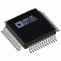
ADUC831BS Analog Devices Inc, ADUC831BS Datasheet - Page 23

ADUC831BS
Manufacturer Part Number
ADUC831BS
Description
IC ADC/DAC 12BIT W/MCU 52-MQFP
Manufacturer
Analog Devices Inc
Series
MicroConverter® ADuC8xxr
Datasheet
1.EVAL-ADUC831QSZ.pdf
(76 pages)
Specifications of ADUC831BS
Rohs Status
RoHS non-compliant
Core Processor
8052
Core Size
8-Bit
Speed
16MHz
Connectivity
EBI/EMI, I²C, SPI, UART/USART
Peripherals
PSM, Temp Sensor, WDT
Number Of I /o
34
Program Memory Size
62KB (62K x 8)
Program Memory Type
FLASH
Eeprom Size
4K x 8
Ram Size
2.25K x 8
Voltage - Supply (vcc/vdd)
2.7 V ~ 5.5 V
Data Converters
A/D 8x12b, D/A 2x12b
Oscillator Type
Internal
Operating Temperature
-40°C ~ 125°C
Package / Case
52-MQFP, 52-PQFP
For Use With
EVAL-ADUC831QSZ - KIT DEV FOR ADUC831 QUICK START
Available stocks
Company
Part Number
Manufacturer
Quantity
Price
Company:
Part Number:
ADUC831BS
Manufacturer:
SHARP
Quantity:
21 512
Company:
Part Number:
ADUC831BS
Manufacturer:
ADI
Quantity:
150
Part Number:
ADUC831BS
Manufacturer:
ADI/亚德诺
Quantity:
20 000
Company:
Part Number:
ADUC831BSB20
Manufacturer:
MINI
Quantity:
892
Company:
Part Number:
ADUC831BSZ
Manufacturer:
Analog Devices Inc
Quantity:
10 000
Part Number:
ADUC831BSZ
Manufacturer:
AD
Quantity:
20 000
Company:
Part Number:
ADUC831BSZ-REEL
Manufacturer:
AD
Quantity:
1 200
Company:
Part Number:
ADUC831BSZ-REEL
Manufacturer:
Analog Devices Inc
Quantity:
10 000
Keep in mind that the ADC’s transfer function is 0 to V
any signal range lost to amplifier saturation near ground will
impact dynamic range. Though the op amps in Table VI are
capable of delivering output signals very closely approaching
ground, no amplifier can deliver signals all the way to ground when
powered by a single supply. Therefore, if a negative supply is
available, you might consider using it to power the front end
amplifiers. If you do, however, be sure to include the Schottky
diodes shown in Figure 10 (or at least the lower of the two
diodes) to protect the analog input from undervoltage condi-
tions. To summarize this section, use the circuit of Figure 10 to
drive the analog input pins of the ADuC831.
Voltage Reference Connections
The on-chip 2.5 V band gap voltage reference can be used as the
reference source for the ADC and DACs. To ensure the accu-
racy of the voltage reference, you must decouple the V
ground with a 0.1 µF capacitor and the C
a 0.1 µF capacitor as shown in Figure 11.
If the internal voltage reference is to be used as a reference for
external circuitry, the C
buffer must be used in this case to ensure that no current is
drawn from the C
that of an internal node within the buffer block, and its voltage
is critical to ADC and DAC accuracy. On the ADuC812 V
was the recommended output for the external reference; this
can be used but it should be noted that there will be a gain error
between this reference and that of the ADC.
The ADuC831 powers up with its internal voltage reference in
the “on” state. This is available at the V
before there will be a gain error between this and that of the
ADC. The C
powered up.
If an external voltage reference is preferred, it should be
connected to the V
Bit 6 of the ADCCON1 SFR must be set to 1 to switch in the
external reference voltage.
REV. 0
BUFFER
Figure 11. Decoupling V
REF
output becomes available when the ADC is
V
REF
REF
REF
0.1 F
0.1 F
C
REF
pin itself. The voltage on the C
and C
REF
output should be used. However, a
REF
51
BUFFER
pins as shown in Figure 12.
REFERENCE
ADuC831
BAND GAP
REF
2.5V
REF
REF
and C
pin, but as noted
pin to ground with
REF
REF
REF
REF
pin is
pin to
REF
, and
–23–
To ensure accurate ADC operation, the voltage applied to V
must be between 1 V and AV
input signals are proportional to the power supply (such as some
strain gage applications) it may be desirable to connect the C
and V
Operation of the ADC or DACs with a reference voltage below
1 V, however, may incur loss of accuracy eventually resulting in
missing codes or non-monotonicity. For that reason, do not use
a reference voltage less than 1 V.
To maintain compatibility with the ADuC812, the external
reference can also be connected to the V
Figure 13, to overdrive the internal reference. Note this intro-
duces a gain error for the ADC that has to be calibrated out,
thus the previous method is the recommended one for most
users. For this method to work, ADCCON1.6 should be config-
ured to use the internal reference. The external reference will
then overdrive this.
REF
Figure 12. Using an External Voltage Reference
Figure 13. Using an External Voltage Reference
REFERENCE
pins directly to AV
REFERENCE
EXTERNAL
EXTERNAL
VOLTAGE
VOLTAGE
V
V
DD
DD
0.1 F
0.1 F
0.1 F
V
C
0.1 F
REF
REF
V
C
REF
REF
51
"1" =
"0" = INTERNAL
DD
DD
.
ADCCON1.6
EXTERNAL
. In situations where analog
51
REFERENCE
BAND GAP
BUFFER
ADuC831
2.5V
ADuC831
REF
REFERENCE
BAND GAP
pin as shown in
2.5V
ADuC831
BUFFER
REF
REF


