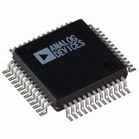
ADUC831BS Analog Devices Inc, ADUC831BS Datasheet - Page 32

ADUC831BS
Manufacturer Part Number
ADUC831BS
Description
IC ADC/DAC 12BIT W/MCU 52-MQFP
Manufacturer
Analog Devices Inc
Series
MicroConverter® ADuC8xxr
Datasheet
1.EVAL-ADUC831QSZ.pdf
(76 pages)
Specifications of ADUC831BS
Rohs Status
RoHS non-compliant
Core Processor
8052
Core Size
8-Bit
Speed
16MHz
Connectivity
EBI/EMI, I²C, SPI, UART/USART
Peripherals
PSM, Temp Sensor, WDT
Number Of I /o
34
Program Memory Size
62KB (62K x 8)
Program Memory Type
FLASH
Eeprom Size
4K x 8
Ram Size
2.25K x 8
Voltage - Supply (vcc/vdd)
2.7 V ~ 5.5 V
Data Converters
A/D 8x12b, D/A 2x12b
Oscillator Type
Internal
Operating Temperature
-40°C ~ 125°C
Package / Case
52-MQFP, 52-PQFP
For Use With
EVAL-ADUC831QSZ - KIT DEV FOR ADUC831 QUICK START
Available stocks
Company
Part Number
Manufacturer
Quantity
Price
Company:
Part Number:
ADUC831BS
Manufacturer:
SHARP
Quantity:
21 512
Company:
Part Number:
ADUC831BS
Manufacturer:
ADI
Quantity:
150
Part Number:
ADUC831BS
Manufacturer:
ADI/亚德诺
Quantity:
20 000
Company:
Part Number:
ADUC831BSB20
Manufacturer:
MINI
Quantity:
892
Company:
Part Number:
ADUC831BSZ
Manufacturer:
Analog Devices Inc
Quantity:
10 000
Part Number:
ADUC831BSZ
Manufacturer:
AD
Quantity:
20 000
Company:
Part Number:
ADUC831BSZ-REEL
Manufacturer:
AD
Quantity:
1 200
Company:
Part Number:
ADUC831BSZ-REEL
Manufacturer:
Analog Devices Inc
Quantity:
10 000
ADuC831
USER INTERFACE TO OTHER ON-CHIP ADuC831
PERIPHERALS
The following section gives a brief overview of the various
peripherals also available on-chip. A summary of the SFRs
used to control and configure these peripherals is also given.
DAC
The ADuC831 incorporates two 12-bit, voltage output DACs
on-chip. Each has a rail-to-rail voltage output buffer capable of
driving 10 kΩ/100 pF. Each has two selectable ranges, 0 V to
V
Each can operate in 12-bit or 8-bit mode. Both DACs share a
control register, DACCON, and four data registers, DAC1H/L,
DACxH/L
Function
SFR Address
Power-On Default Value
Bit Addressable
The 12-bit DAC data should be written into DACxH/L right-justified such that DACxL contains the lower eight bits, and the lower
nibble of DACxH contains the upper four bits.
Bit
7
6
5
4
3
2
1
0
REF
(the internal band gap 2.5 V reference) and 0 V to AV
Name
MODE
RNG1
RNG0
CLR1
CLR0
SYNC
PD1
PD0
The DAC MODE bit sets the overriding operating mode for both DACs.
DAC1 Range Select Bit.
DAC0 Range Select Bit.
DAC0 Power-Down Bit.
Description
Set to “1” = 8-Bit Mode (Write 8 Bits to DACxL SFR).
Set to “0”= 12-Bit Mode.
Set to “1” = DAC1 Range 0–V
Set to “0” = DAC1 Range 0–V
Set to “1” = DAC0 Range 0–V
Set to “0” = DAC0 Range 0–V
DAC1 Clear Bit.
Set to “0” = DAC1 Output Forced to 0 V.
Set to “1” = DAC1 Output Normal.
DAC0 Clear Bit.
Set to “0” = DAC1 Output Forced to 0 V.
Set to “1” = DAC1 Output Normal.
DAC0/1 Update Synchronization Bit.
When set to “1” the DAC outputs update as soon as DACxL SFRs are written. The user can
simultaneously update both DACs by first updating the DACxL/H SFRs while SYNC is “0.” Both
DACs will then update simultaneously when the SYNC bit is set to “1.”
DAC1 Power-Down Bit.
Set to “1” = Power-On DAC1.
Set to “0” = Power-Off DAC1.
Set to “1” = Power-On DAC0.
Set to “0” = Power-Off DAC0.
DAC Data Registers
DAC Data Registers, written by user to update the DAC output.
DAC0L (DAC0 Data Low Byte)
DAC0H (DAC0 Data High Byte)
00H
No
Table IX. DACCON SFR Bit Designations
DD
REF
DD.
REF.
DD
.
.
.
–32–
DAC0H/L. It should be noted that in 12-bit asynchronous
mode, the DAC voltage output will be updated as soon as the
DACL data SFR has been written; therefore, the DAC data
registers should be updated as DACH first, followed by DACL.
Note: for correct DAC operation on the 0 to V
ADC must be switched on. This results in the DAC using the
correct reference value.
DACCON
SFR Address
Power-On Default Value
Bit Addressable
F9H; DAC1L (DAC1 Data Low Byte)
FAH; DAC1H(DAC1 Data High Byte)
All four Registers
All four Registers
DAC Control Register
FDH
04H
No
REF
FBH
FCH
range, the
REV. 0


