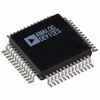
ADUC831BS Analog Devices Inc, ADUC831BS Datasheet - Page 27

ADUC831BS
Manufacturer Part Number
ADUC831BS
Description
IC ADC/DAC 12BIT W/MCU 52-MQFP
Manufacturer
Analog Devices Inc
Series
MicroConverter® ADuC8xxr
Datasheet
1.EVAL-ADUC831QSZ.pdf
(76 pages)
Specifications of ADUC831BS
Rohs Status
RoHS non-compliant
Core Processor
8052
Core Size
8-Bit
Speed
16MHz
Connectivity
EBI/EMI, I²C, SPI, UART/USART
Peripherals
PSM, Temp Sensor, WDT
Number Of I /o
34
Program Memory Size
62KB (62K x 8)
Program Memory Type
FLASH
Eeprom Size
4K x 8
Ram Size
2.25K x 8
Voltage - Supply (vcc/vdd)
2.7 V ~ 5.5 V
Data Converters
A/D 8x12b, D/A 2x12b
Oscillator Type
Internal
Operating Temperature
-40°C ~ 125°C
Package / Case
52-MQFP, 52-PQFP
For Use With
EVAL-ADUC831QSZ - KIT DEV FOR ADUC831 QUICK START
Available stocks
Company
Part Number
Manufacturer
Quantity
Price
Company:
Part Number:
ADUC831BS
Manufacturer:
SHARP
Quantity:
21 512
Company:
Part Number:
ADUC831BS
Manufacturer:
ADI
Quantity:
150
Part Number:
ADUC831BS
Manufacturer:
ADI/亚德诺
Quantity:
20 000
Company:
Part Number:
ADUC831BSB20
Manufacturer:
MINI
Quantity:
892
Company:
Part Number:
ADUC831BSZ
Manufacturer:
Analog Devices Inc
Quantity:
10 000
Part Number:
ADUC831BSZ
Manufacturer:
AD
Quantity:
20 000
Company:
Part Number:
ADUC831BSZ-REEL
Manufacturer:
AD
Quantity:
1 200
Company:
Part Number:
ADUC831BSZ-REEL
Manufacturer:
Analog Devices Inc
Quantity:
10 000
NONVOLATILE FLASH/EE MEMORY
Flash/EE Memory Overview
The ADuC831 incorporates Flash/EE memory technology on-chip
to provide the user with nonvolatile, in-circuit reprogrammable
code, and data memory space. Flash/EE memory is a relatively
recent type of nonvolatile memory technology and is based on a
single transistor cell architecture.
This technology is basically an outgrowth of EPROM technology
and was developed through the late 1980s. Flash/EE memory
takes the flexible in-circuit reprogrammable features of EEPROM
and combines them with the space efficient/density features of
EPROM (see Figure 17).
Because Flash/EE technology is based on a single transistor cell
architecture, a Flash memory array, like EPROM, can be imple-
mented to achieve the space efficiencies or memory densities
required by a given design. Like EEPROM, Flash memory can
be programmed in-system at a byte level, although it must first be
erased; the erase being performed in page blocks. Thus, Flash
memory is often and more correctly referred to as Flash/EE memory.
Overall, Flash/EE memory represents a step closer to the ideal
memory device that includes nonvolatility, in-circuit programma-
bility, high density and low cost. Incorporated in the ADuC831,
Flash/EE memory technology allows the user to update program
code space in-circuit, without the need to replace onetime
programmable (OTP) devices at remote operating nodes.
Flash/EE Memory and the ADuC831
The ADuC831 provides two arrays of Flash/EE memory for user
applications. 62 kBytes of Flash/EE program space are provided
on-chip to facilitate code execution without any external dis-
crete ROM device requirements. The program memory can be
programmed in-circuit using the serial download mode provided,
using conventional third party memory programmers, or via a
user defined protocol that can configure it as data if required.
A 4 kByte Flash/EE data memory space is also provided on-chip.
This may be used as a general-purpose nonvolatile scratchpad
area. User access to this area is via a group of six SFRs. This
space can be programmed at a byte level, although it must first
be erased in 4-byte pages.
ADuC831 Flash/EE Memory Reliability
The Flash/EE program and data memory arrays on the ADuC831
are fully qualified for two key Flash/EE memory characteristics,
namely Flash/EE Memory Cycling Endurance and Flash/EE
Memory Data Retention.
REV. 0
SPACE EFFICIENT/
Figure 17. Flash/EE Memory Development
DENSITY
TECHNOLOGY
EPROM
FLASH/EE MEMORY
TECHNOLOGY
TECHNOLOGY
REPROGRAMMABLE
EEPROM
IN-CIRCUIT
–27–
Endurance quantifies the ability of the Flash/EE memory to be
cycled through many program, read, and erase cycles. In real
terms, a single endurance cycle is composed of four indepen-
dent, sequential events. These events are defined as:
In reliability qualification, every byte in both the program and
data Flash/EE memory is cycled from 00H to FFH until a first
fail is recorded, signifying the endurance limit of the on-chip
Flash/EE memory.
As indicated in the specification pages of this data sheet, the
ADuC831 Flash/EE Memory Endurance qualification has been
carried out in accordance with JEDEC Specification A117 over
the industrial temperature range of –40°C to +25°C and +85°C
to +125°C. The results allow the specification of a minimum
endurance figure over supply and temperature of 100,000
cycles, with an endurance figure of 700,000 cycles being typical
of operation at 25°C.
Retention quantifies the ability of the Flash/EE memory to
retain its programmed data over time. Again, the ADuC831 has
been qualified in accordance with the formal JEDEC Retention
Lifetime Specification (A117) at a specific junction temperature
(T
memory is cycled to its specified endurance limit described above
before data retention is characterized. This means that the
Flash/EE memory is guaranteed to retain its data for its full
specified retention lifetime every time the Flash/EE memory is
reprogrammed. It should also be noted that retention lifetime,
based on an activation energy of 0.6 eV, will derate with T
shown in Figure 18.
a. Initial page erase sequence
b. Read/verify sequence
c. Byte program sequence
d. Second read/verify sequence
J
= 55°C). As part of this qualification procedure, the Flash/EE
300
250
200
150
100
Figure 18. Flash/EE Memory Data Retention
50
0
40
50
T
J
60
JUNCTION TEMPERATURE – C
ADI SPECIFICATION
100 YEARS MIN.
AT T
70
J
= 55 C
80
A single Flash/EE
Memory
Endurance Cycle
90
ADuC831
100
110
J
as


