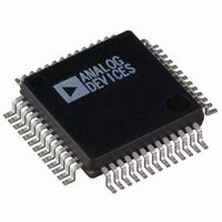
ADUC831BS Analog Devices Inc, ADUC831BS Datasheet - Page 47

ADUC831BS
Manufacturer Part Number
ADUC831BS
Description
IC ADC/DAC 12BIT W/MCU 52-MQFP
Manufacturer
Analog Devices Inc
Series
MicroConverter® ADuC8xxr
Datasheet
1.EVAL-ADUC831QSZ.pdf
(76 pages)
Specifications of ADUC831BS
Rohs Status
RoHS non-compliant
Core Processor
8052
Core Size
8-Bit
Speed
16MHz
Connectivity
EBI/EMI, I²C, SPI, UART/USART
Peripherals
PSM, Temp Sensor, WDT
Number Of I /o
34
Program Memory Size
62KB (62K x 8)
Program Memory Type
FLASH
Eeprom Size
4K x 8
Ram Size
2.25K x 8
Voltage - Supply (vcc/vdd)
2.7 V ~ 5.5 V
Data Converters
A/D 8x12b, D/A 2x12b
Oscillator Type
Internal
Operating Temperature
-40°C ~ 125°C
Package / Case
52-MQFP, 52-PQFP
For Use With
EVAL-ADUC831QSZ - KIT DEV FOR ADUC831 QUICK START
Available stocks
Company
Part Number
Manufacturer
Quantity
Price
Company:
Part Number:
ADUC831BS
Manufacturer:
SHARP
Quantity:
21 512
Company:
Part Number:
ADUC831BS
Manufacturer:
ADI
Quantity:
150
Part Number:
ADUC831BS
Manufacturer:
ADI/亚德诺
Quantity:
20 000
Company:
Part Number:
ADUC831BSB20
Manufacturer:
MINI
Quantity:
892
Company:
Part Number:
ADUC831BSZ
Manufacturer:
Analog Devices Inc
Quantity:
10 000
Part Number:
ADUC831BSZ
Manufacturer:
AD
Quantity:
20 000
Company:
Part Number:
ADUC831BSZ-REEL
Manufacturer:
AD
Quantity:
1 200
Company:
Part Number:
ADUC831BSZ-REEL
Manufacturer:
Analog Devices Inc
Quantity:
10 000
8052 COMPATIBLE ON-CHIP PERIPHERALS
This section gives a brief overview of the various secondary
peripheral circuits that are also available to the user on-chip.
These remaining functions are mostly 8052 compatible (with a
few additional features) and are controlled via standard 8052
SFR bit definitions.
Parallel I/O
The ADuC831 uses four input/output ports to exchange data
with external devices. In addition to performing general-purpose
I/O, some ports are capable of external memory operations while
others are multiplexed with alternate functions for the peripheral
features on the device. In general, when a peripheral is enabled,
that pin may not be used as a general-purpose I/O pin.
Port 0
Port 0 is an 8-bit, open-drain, bidirectional I/O port that is directly
controlled via the Port 0 SFR. Port 0 is also the multiplexed
low-order address and data bus during accesses to external pro-
gram or data memory.
Figure 36 shows a typical bit latch and I/O buffer for a Port 0
port pin. The bit latch (one bit in the port’s SFR) is represented
as a Type D flip-flop, which will clock in a value from the inter-
nal bus in response to a “write to latch” signal from the CPU.
The Q output of the flip-flop is placed on the internal bus in
response to a “read latch” signal from the CPU. The level of the
port pin itself is placed on the internal bus in response to a
“read pin” signal from the CPU. Some instructions that read a
port activate the “read latch” signal, and others activate the
“read pin” signal. See the following Read-Modify-Write Instruc-
tions section for more details.
As shown in Figure 36, the output drivers of Port 0 pins are
switchable to an internal ADDR and ADDR/DATA bus by an
internal CONTROL signal for use in external memory accesses.
During external memory accesses the P0 SFR gets 1s written to it
(i.e., all of its bit latches become 1). When accessing external
memory, the CONTROL signal in Figure 36 goes high, enabling
push-pull operation of the output pin from the internal address or
data bus (ADDR/DATA line). Therefore, no external pull-ups are
required on Port 0 in order for it to access external memory.
REV. 0
INTERNAL
TO LATCH
LATCH
Figure 36. Port 0 Bit Latch and I/O Buffer
WRITE
READ
READ
BUS
PIN
LATCH
D
CL
Q
Q
ADDR/DATA
CONTROL
DV
DD
P0.x
PIN
–47–
In general-purpose I/O port mode, Port 0 pins that have 1s written
to them via the Port 0 SFR will be configured as “open drain”
and will therefore float. In this state, Port 0 pins can be used as
high impedance inputs. This is represented in Figure 36 by the
NAND gate whose output remains high as long as the CONTROL
signal is low, thereby disabling the top FET. External pull-up
resistors are therefore required when Port 0 pins are used as
general-purpose outputs. Port 0 pins with 0s written to them
will drive a logic low output voltage (V
sinking 1.6 mA.
Port 1
Port 1 is also an 8-bit port directly controlled via the P1 SFR.
Port 1 digital output capability is not supported on this device.
Port 1 pins can be configured as digital inputs or analog inputs.
By (power-on) default these pins are configured as analog
inputs, i.e., 1 written in the corresponding Port 1 register bit.
To configure any of these pins as digital inputs, the user should
write a 0 to these port bits to configure the corresponding pin as
a high impedance digital input.
These pins also have various secondary functions described in
Table XVII.
Pin
P1.0
P1.1
P1.5
Port 2
Port 2 is a bidirectional port with internal pull-up resistors
directly controlled via the P2 SFR. Port 2 also emits the high
order address bytes during fetches from external program memory
and middle and high order address bytes during accesses to the
24-bit external data memory space.
As shown in Figure 38, the output drivers of Ports 2 are switchable
to an internal ADDR and ADDR/DATA bus by an internal
CONTROL signal for use in external memory accesses (as for
Port 0). In external memory addressing mode (CONTROL = 1)
the port pins feature push-pull operation controlled by the inter-
nal address bus (ADDR line). However, unlike the P0 SFR
during external memory accesses, the P2 SFR remains unchanged.
Table XVII. Port 1, Alternate Pin Functions
Figure 37. Port 1 Bit Latch and I/O Buffer
INTERNAL
TO LATCH
Alternate Function
T2 (Timer/Counter 2 External Input)
T2EX (Timer/Counter 2 Capture/Reload Trigger)
SS (Slave Select for the SPI Interface)
LATCH
WRITE
READ
READ
BUS
PIN
TO ADC
LATCH
D
CL
Q
Q
OL
) and will be capable of
ADuC831
P1.x
PIN


