HD64F3694FY Renesas Electronics America, HD64F3694FY Datasheet - Page 11
HD64F3694FY
Manufacturer Part Number
HD64F3694FY
Description
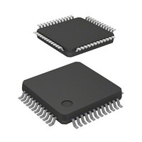
IC H8 MCU FLASH 32K 48-LQFP
Manufacturer
Renesas Electronics America
Series
H8® H8/300H Tinyr
Datasheet
1.HD64F3694GFYV.pdf
(452 pages)
Specifications of HD64F3694FY
Core Processor
H8/300H
Core Size
16-Bit
Speed
20MHz
Connectivity
I²C, SCI
Peripherals
PWM, WDT
Number Of I /o
29
Program Memory Size
32KB (32K x 8)
Program Memory Type
FLASH
Ram Size
2K x 8
Voltage - Supply (vcc/vdd)
3 V ~ 5.5 V
Data Converters
A/D 8x10b
Oscillator Type
Internal
Operating Temperature
-20°C ~ 75°C
Package / Case
48-LQFP
Lead Free Status / RoHS Status
Contains lead / RoHS non-compliant
Eeprom Size
-
Available stocks
Company
Part Number
Manufacturer
Quantity
Price

Part Number:
HD64F3694FYJV
Manufacturer:
RENESAS/瑞萨
Quantity:
20 000
Company:
Part Number:
HD64F3694FYV
Manufacturer:
Renesas Electronics America
Quantity:
10 000


Section 1 Overview................................................................................................1
1.1
1.2
1.3
1.4
Section 2 CPU......................................................................................................13
2.1
2.2
2.3
2.4
2.5
2.6
2.7
2.8
Section 3 Exception Handling .............................................................................49
3.1
3.2
Features.................................................................................................................................. 1
Internal Block Diagram.......................................................................................................... 4
Pin Arrangement .................................................................................................................... 6
Pin Functions ......................................................................................................................... 9
Address Space and Memory Map ........................................................................................ 14
Register Configuration......................................................................................................... 17
2.2.1
2.2.2
2.2.3
Data Formats........................................................................................................................ 21
2.3.1
2.3.2
Instruction Set ...................................................................................................................... 24
2.4.1
2.4.2
Addressing Modes and Effective Address Calculation........................................................ 34
2.5.1
2.5.2
Basic Bus Cycle ................................................................................................................... 40
2.6.1
2.6.2
CPU States ........................................................................................................................... 42
Usage Notes ......................................................................................................................... 43
2.8.1
2.8.2
2.8.3
Exception Sources and Vector Address ............................................................................... 49
Register Descriptions ........................................................................................................... 51
3.2.1
3.2.2
3.2.3
3.2.4
General Registers.................................................................................................... 18
Program Counter (PC) ............................................................................................ 19
Condition-Code Register (CCR)............................................................................. 19
General Register Data Formats ............................................................................... 21
Memory Data Formats ............................................................................................ 23
Table of Instructions Classified by Function .......................................................... 24
Basic Instruction Formats ....................................................................................... 33
Addressing Modes .................................................................................................. 34
Effective Address Calculation ................................................................................ 38
Access to On-Chip Memory (RAM, ROM)............................................................ 40
On-Chip Peripheral Modules .................................................................................. 41
Notes on Data Access to Empty Areas ................................................................... 43
EEPMOV Instruction.............................................................................................. 43
Bit Manipulation Instruction................................................................................... 43
Interrupt Edge Select Register 1 (IEGR1) .............................................................. 51
Interrupt Edge Select Register 2 (IEGR2) .............................................................. 52
Interrupt Enable Register 1 (IENR1) ...................................................................... 53
Interrupt Flag Register 1 (IRR1)............................................................................. 54
Contents
Rev.5.00 Nov. 02, 2005 Page ix of xxviii
Related parts for HD64F3694FY
Image
Part Number
Description
Manufacturer
Datasheet
Request
R

Part Number:
Description:
(HD64 Series) Hitachi Single-Chip Microcomputer
Manufacturer:
Hitachi Semiconductor
Datasheet:

Part Number:
Description:
KIT STARTER FOR M16C/29
Manufacturer:
Renesas Electronics America
Datasheet:

Part Number:
Description:
KIT STARTER FOR R8C/2D
Manufacturer:
Renesas Electronics America
Datasheet:

Part Number:
Description:
R0K33062P STARTER KIT
Manufacturer:
Renesas Electronics America
Datasheet:

Part Number:
Description:
KIT STARTER FOR R8C/23 E8A
Manufacturer:
Renesas Electronics America
Datasheet:

Part Number:
Description:
KIT STARTER FOR R8C/25
Manufacturer:
Renesas Electronics America
Datasheet:

Part Number:
Description:
KIT STARTER H8S2456 SHARPE DSPLY
Manufacturer:
Renesas Electronics America
Datasheet:

Part Number:
Description:
KIT STARTER FOR R8C38C
Manufacturer:
Renesas Electronics America
Datasheet:

Part Number:
Description:
KIT STARTER FOR R8C35C
Manufacturer:
Renesas Electronics America
Datasheet:

Part Number:
Description:
KIT STARTER FOR R8CL3AC+LCD APPS
Manufacturer:
Renesas Electronics America
Datasheet:
Part Number:
Description:
KIT STARTER FOR RX610
Manufacturer:
Renesas Electronics America
Datasheet:

Part Number:
Description:
KIT STARTER FOR R32C/118
Manufacturer:
Renesas Electronics America
Datasheet:

Part Number:
Description:
KIT DEV RSK-R8C/26-29
Manufacturer:
Renesas Electronics America
Datasheet:

Part Number:
Description:
KIT STARTER FOR SH7124
Manufacturer:
Renesas Electronics America
Datasheet:

Part Number:
Description:
KIT STARTER FOR H8SX/1622
Manufacturer:
Renesas Electronics America
Datasheet: