HD64F3694FY Renesas Electronics America, HD64F3694FY Datasheet - Page 24
HD64F3694FY
Manufacturer Part Number
HD64F3694FY
Description
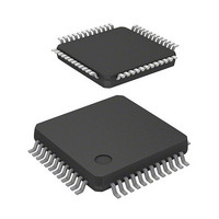
IC H8 MCU FLASH 32K 48-LQFP
Manufacturer
Renesas Electronics America
Series
H8® H8/300H Tinyr
Datasheet
1.HD64F3694GFYV.pdf
(452 pages)
Specifications of HD64F3694FY
Core Processor
H8/300H
Core Size
16-Bit
Speed
20MHz
Connectivity
I²C, SCI
Peripherals
PWM, WDT
Number Of I /o
29
Program Memory Size
32KB (32K x 8)
Program Memory Type
FLASH
Ram Size
2K x 8
Voltage - Supply (vcc/vdd)
3 V ~ 5.5 V
Data Converters
A/D 8x10b
Oscillator Type
Internal
Operating Temperature
-20°C ~ 75°C
Package / Case
48-LQFP
Lead Free Status / RoHS Status
Contains lead / RoHS non-compliant
Eeprom Size
-
Available stocks
Company
Part Number
Manufacturer
Quantity
Price

Part Number:
HD64F3694FYJV
Manufacturer:
RENESAS/瑞萨
Quantity:
20 000
Company:
Part Number:
HD64F3694FYV
Manufacturer:
Renesas Electronics America
Quantity:
10 000


Section 14 Serial Communication Interface 3 (SCI3)
Figure 14.1 Block Diagram of SCI3........................................................................................... 190
Figure 14.2 Data Format in Asynchronous Communication ...................................................... 205
Figure 14.3 Relationship between Output Clock and Transfer Data Phase
Figure 14.4 Sample SCI3 Initialization Flowchart ..................................................................... 206
Figure 14.5 Example SCI3 Operation in Transmission in Asynchronous Mode
Figure 14.6 Sample Serial Transmission Flowchart (Asynchronous Mode) .............................. 208
Figure 14.7 Example SCI3 Operation in Reception in Asynchronous Mode
Figure 14.8 Sample Serial Data Reception Flowchart (Asynchronous mode) (1)...................... 211
Figure 14.8 Sample Serial Reception Data Flowchart (2) .......................................................... 212
Figure 14.9 Data Format in Clocked Synchronous Communication .......................................... 213
Figure 14.10 Example of SCI3 Operation in Transmission in Clocked Synchronous Mode...... 215
Figure 14.11 Sample Serial Transmission Flowchart (Clocked Synchronous Mode) ................ 216
Figure 14.12 Example of SCI3 Reception Operation in Clocked Synchronous Mode............... 217
Figure 14.13 Sample Serial Reception Flowchart (Clocked Synchronous Mode)...................... 218
Figure 14.14 Sample Flowchart of Simultaneous Serial Transmit
Figure 14.15 Example of Communication Using Multiprocessor Format
Figure 14.16 Sample Multiprocessor Serial Transmission Flowchart ........................................ 223
Figure 14.17 Sample Multiprocessor Serial Reception Flowchart (1)........................................ 225
Figure 14.17 Sample Multiprocessor Serial Reception Flowchart (2)........................................ 226
Figure 14.18 Example of SCI3 Operation in Reception Using Multiprocessor Format
Figure 14.19 Receive Data Sampling Timing in Asynchronous Mode ...................................... 230
Section 15 I
Figure 15.1 Block Diagram of I
Figure 15.2 External Circuit Connections of I/O Pins ................................................................ 233
Figure 15.3 I
Figure 15.4 I
Figure 15.5 Master Transmit Mode Operation Timing (1)......................................................... 248
Figure 15.6 Master Transmit Mode Operation Timing (2)......................................................... 248
Figure 15.7 Master Receive Mode Operation Timing (1) .......................................................... 250
Figure 15.8 Master Receive Mode Operation Timing (2) .......................................................... 251
Figure 15.9 Slave Transmit Mode Operation Timing (1) ........................................................... 252
Figure 15.10 Slave Transmit Mode Operation Timing (2) ......................................................... 253
Rev.5.00 Nov. 02, 2005 Page xxii of xxviii
(Asynchronous Mode) (Example with 8-Bit Data, Parity, Two Stop Bits) ............. 205
(8-Bit Data, Parity, One Stop Bit) ........................................................................... 207
(8-Bit Data, Parity, One Stop Bit) ........................................................................... 209
2
2
2
(Example with 8-Bit Data, Multiprocessor Bit, One Stop Bit) .............................. 227
and Receive Operations (Clocked Synchronous Mode) ........................................ 220
(Transmission of Data H'AA to Receiving Station A) .......................................... 222
C Bus Interface 2 (IIC2)
C Bus Formats ...................................................................................................... 246
C Bus Timing........................................................................................................ 246
2
C Bus Interface 2..................................................................... 232
Related parts for HD64F3694FY
Image
Part Number
Description
Manufacturer
Datasheet
Request
R

Part Number:
Description:
(HD64 Series) Hitachi Single-Chip Microcomputer
Manufacturer:
Hitachi Semiconductor
Datasheet:

Part Number:
Description:
KIT STARTER FOR M16C/29
Manufacturer:
Renesas Electronics America
Datasheet:

Part Number:
Description:
KIT STARTER FOR R8C/2D
Manufacturer:
Renesas Electronics America
Datasheet:

Part Number:
Description:
R0K33062P STARTER KIT
Manufacturer:
Renesas Electronics America
Datasheet:

Part Number:
Description:
KIT STARTER FOR R8C/23 E8A
Manufacturer:
Renesas Electronics America
Datasheet:

Part Number:
Description:
KIT STARTER FOR R8C/25
Manufacturer:
Renesas Electronics America
Datasheet:

Part Number:
Description:
KIT STARTER H8S2456 SHARPE DSPLY
Manufacturer:
Renesas Electronics America
Datasheet:

Part Number:
Description:
KIT STARTER FOR R8C38C
Manufacturer:
Renesas Electronics America
Datasheet:

Part Number:
Description:
KIT STARTER FOR R8C35C
Manufacturer:
Renesas Electronics America
Datasheet:

Part Number:
Description:
KIT STARTER FOR R8CL3AC+LCD APPS
Manufacturer:
Renesas Electronics America
Datasheet:
Part Number:
Description:
KIT STARTER FOR RX610
Manufacturer:
Renesas Electronics America
Datasheet:

Part Number:
Description:
KIT STARTER FOR R32C/118
Manufacturer:
Renesas Electronics America
Datasheet:

Part Number:
Description:
KIT DEV RSK-R8C/26-29
Manufacturer:
Renesas Electronics America
Datasheet:

Part Number:
Description:
KIT STARTER FOR SH7124
Manufacturer:
Renesas Electronics America
Datasheet:

Part Number:
Description:
KIT STARTER FOR H8SX/1622
Manufacturer:
Renesas Electronics America
Datasheet: