FAN1581DX Fairchild Semiconductor, FAN1581DX Datasheet - Page 6
FAN1581DX
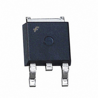
Manufacturer Part Number
FAN1581DX
Description
IC REG LDO 5A ADJ VOLT TO-252
Manufacturer
Fairchild Semiconductor
Datasheet
1.FAN1581M25X.pdf
(13 pages)
Specifications of FAN1581DX
Regulator Topology
Positive Adjustable
Voltage - Output
1.25 ~ 5.7 V
Voltage - Input
Up to 7V
Voltage - Dropout (typical)
0.4V @ 5A
Number Of Regulators
1
Current - Output
5A
Current - Limit (min)
5.2A
Operating Temperature
0°C ~ 125°C
Mounting Type
Surface Mount
Package / Case
TO-252-2, DPak (2 Leads + Tab), TO-252AA, SC-63
Lead Free Status / RoHS Status
Lead free / RoHS Compliant


FAN1581
General
The FAN1581, FAN1581-1.2, FAN1581-1.5, and
FAN1581-2.5 are three-terminal regulators optimized for
DDR and GTL+ V
These devices are short-circuit protected, and offer thermal
shutdown to turn off the regulator when the junction temper-
ature exceeds about 150°C. The FAN1581 series provides
low dropout voltage and fast transient response. Frequency
compensation uses capacitors with low ESR while still main-
taining stability. This is critical in addressing the needs of
low voltage high speed microprocessor buses like GTL+.
V
The FAN1581 utilizes a dual supply approach to maximize
efficiency. The collector of the power device is brought out
to the V
high current loads. V
circuitry and the drive for the output NPN transistor.
V
age. Special care was taken to ensure there are no supply-
sequencing problems. The output voltage will not turn on
until both supplies are operating. If the control voltage
comes up first, the output current will be typically limited to
about 3.0mA until the power input voltage comes up. If the
power input voltage comes up first the output will not turn
on at all until the control voltage comes up. The output can
never come up unregulated.
The FAN1581 can also be used as a single supply device
with the control and power inputs tied together. In this mode,
the dropout is determined by the minimum control voltage.
Stability
The FAN1581 series requires an output capacitor as a part of
the frequency compensation. It is recommended to use a 22µF
solid tantalum or a 100µF aluminum electrolytic on the output
to ensure stability. The frequency compensation of these
devices optimizes the frequency response with low ESR capaci-
tors. In general, it is suggested to use capacitors with an ESR
of < 0.3Ω. It is also recommended to use bypass capacitors
such as a 22µF tantalum or a 100µF aluminum on the
adjust pin of the FAN1581 for low ripple and fast transient
response. When these bypassing capacitors are not used at the
adjust pin, smaller values of output capacitors provide equally
good results. A graph showing stability of output capacitance
ESR vs. load current can be found under Typical Performance
Characteristics.
Protection Diodes
In normal operation, the FAN1581 series does not require any
protection diodes. For the FAN1581, internal resistors limit
internal current paths on the adjust pin. Therefore, even with
bypass capacitors on the adjust pin, no protection diode is
needed to ensure device safety under short-circuit conditions.
6
CNTL
IN
and V
should be at least 1.2V higher than the output volt-
IN
pin to minimize internal power dissipation under
CNTL
TT
Functions
CNTL
termination and logic applications.
provides power for the control
A protection diode between the input and output pins is
usually not needed. An internal diode between the input and
the output pins on the FAN1581 series can handle microsec-
ond surge currents of 50A to 100A. Even with large value
output capacitors it is difficult to obtain those values of surge
currents in normal operation. Only with large values of out-
put capacitance, such as 1000µF to 5000µF, and with the
input pin instantaneously shorted to ground can damage
occur. A crowbar circuit at the input can generate those levels
of current; a diode from output to input is then recommended,
as shown in Figure 1. Usually, normal power supply cycling
or system “hot plugging and unplugging” will not generate
current large enough to do any damage.
Ripple Rejection
In applications that require improved ripple rejection, a bypass
capacitor from the adjust pin of the FAN1581 to ground
reduces the output ripple by the ratio of V
impedance of the adjust pin capacitor at the ripple frequency
should be less than the value of R1 (typically in the range of
100Ω to 120Ω) in the feedback divider network in Figure 1.
Therefore, the value of the required adjust pin capacitor is a
function of the input ripple frequency. For example, if R1 equals
100Ω and the ripple frequency equals 120Hz, the adjust pin
capacitor should be 22µF. At 10kHz, only 0.22µF is needed.
Output Voltage
The FAN1581 regulator develops a 1.25V reference voltage
between the output pin and the adjust pin (see Figure 2).
Placing a resistor R1 between these two terminals causes a
constant current to flow through R1 and down through R2 to
set the overall output voltage. Normally, this current is the
specified minimum load current of 10mA.
V
V
OUT
CNTL
V
V
IN
IN
+
+
Figure 1. Optional Protection Diode
C1
10μF
C1
10μF
Vcntl
Vin
Vcntl
Vin
(OPTIONAL)
(OPTIONAL)
FAN1581
FAN1581
1N4002
1N4002
Gnd
+
Adj
D1
D1
Vsense
Vsense
C
Vout
Vout
ADJ
PRODUCT SPECIFICATION
+
R1
R2
OUT
C2
22μF
REV. 1.2.1 7/2/09
+
/1.25V. The
C2
22μF
V
V
OUT
OUT
Related parts for FAN1581DX
Image
Part Number
Description
Manufacturer
Datasheet
Request
R

Part Number:
Description:
Fairchild Semiconductor [IGBT MODULE]
Manufacturer:
Fairchild Semiconductor
Datasheet:

Part Number:
Description:
Discrete Semiconductor Modules
Manufacturer:
Fairchild Semiconductor
Part Number:
Description:
Discrete Semiconductor Modules
Manufacturer:
Fairchild Semiconductor
Part Number:
Description:
This N-Channel MOSFET is produced using Fairchild Semiconductor’s advanced Power Trench® process
Manufacturer:
Fairchild Semiconductor
Datasheet:
Part Number:
Description:
This N-Channel MOSFET is produced using Fairchild Semiconductor’s advanced Power Trench® process
Manufacturer:
Fairchild Semiconductor
Datasheet:
Part Number:
Description:
This N-Channel MOSFET is produced using Fairchild Semiconductor’s advanced PowerTrench® process
Manufacturer:
Fairchild Semiconductor
Datasheet:
Part Number:
Description:
This N-Channel MOSFET is produced using Fairchild Semiconductor’s advanced PowerTrench® process
Manufacturer:
Fairchild Semiconductor
Datasheet:
Part Number:
Description:
This N-Channel MOSFET is produced using Fairchild Semiconductor’s advanced Power Trench® process
Manufacturer:
Fairchild Semiconductor
Datasheet:
Part Number:
Description:
This N-Channel logic Level MOSFETs are produced using Fairchild Semiconductor‘s advanced Power Trench® process that has been special tailored to minimize the on-state resistance and yet maintain superior switching performance
Manufacturer:
Fairchild Semiconductor
Datasheet:
Part Number:
Description:
This N-Channel MOSFET is produced using Fairchild Semiconductor’s advanced Power Trench® process
Manufacturer:
Fairchild Semiconductor
Datasheet:
Part Number:
Description:
This N-Channel SyncFET™ is produced using Fairchild Semiconductor’s advanced PowerTrench® process
Manufacturer:
Fairchild Semiconductor
Datasheet:
Part Number:
Description:
This N-Channel SyncFET™ is produced using Fairchild Semiconductor’s advanced PowerTrench® process
Manufacturer:
Fairchild Semiconductor
Datasheet:
Part Number:
Description:
This N-Channel SyncFET™ is produced using Fairchild Semiconductor’s advanced PowerTrench® process
Manufacturer:
Fairchild Semiconductor
Datasheet:
Part Number:
Description:
This N-Channel logic Level MOSFETs are produced using Fairchild Semiconductor‘s advanced Power Trench® process that has been special tailored to minimize the on-state resistance and yet maintain superior switching performance
Manufacturer:
Fairchild Semiconductor
Datasheet:
Part Number:
Description:
This N-Channel MOSFET is produced using Fairchild Semiconductor’s advanced Power Trench® process that has been especially tailored to minimize the on-state resistance and yet maintain superior switching performance
Manufacturer:
Fairchild Semiconductor
Datasheet: