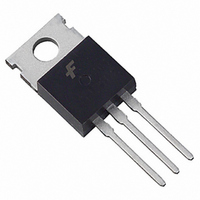
FAN1585AT Fairchild Semiconductor, FAN1585AT Datasheet - Page 7

FAN1585AT
Manufacturer Part Number
FAN1585AT
Description
IC REG LDO 5A ADJ VOLT TO-220
Manufacturer
Fairchild Semiconductor
Datasheet
1.FAN1585AM18X.pdf
(13 pages)
Specifications of FAN1585AT
Regulator Topology
Positive Adjustable
Voltage - Output
1.25 ~ 7 V
Voltage - Input
Up to 18V
Voltage - Dropout (typical)
1.15V @ 5A
Number Of Regulators
1
Current - Output
5A
Current - Limit (min)
5.1A
Operating Temperature
25°C ~ 125°C
Mounting Type
Through Hole
Package / Case
TO-220-3 (Straight Leads)
Lead Free Status / RoHS Status
Lead free / RoHS Compliant
PRODUCT SPECIFICATION
Load Regulation
It is not possible to provide true remote load sensing because
the FAN1585A series are three-terminal devices. Load regu-
lation is limited by the resistance of the wire connecting the
regulators to the load. Load regulation per the data sheet
specification is measured at the bottom of the package.
For fixed voltage devices, negative side sensing is a true
Kelvin connection with the ground pin of the device returned
to the negative side of the load. This is illustrated in Figure 12.
Figure 12. Connection for Best Load Regulation
For adjustable voltage devices, negative side sensing is a true
Kelvin connection with the bottom of the output divider
returned to the negative side of the load. The best load regu-
lation is obtained when the top of the resistor divider R1 con-
nects directly to the regulator output and not to the load.
Figure 13 illustrates this point.
If R1 connects to the load, then the effective resistance
between the regulator and the load would be:
R
The connection shown in Figure 13 does not multiply R
the divider ratio. As an example, R
per foot with 16-gauge wire. This translates to 4mV per foot
at 1A load current. At higher load currents, this drop repre-
sents a significant percentage of the overall regulation. It is
important to keep the positive lead between the regulator and
the load as short as possible and to use large wire or PC
board traces.
REV. 1.1.6 7/8/05
V
V
P
OUT
IN
x (1 + R2/R1), R
+
= V
V
IN
REF
C1
22 F
Figure 11. Basic Regulator Circuit
(1 + R2/R1) + I
IN
FAN1585A-1.5
IN
I
35 A
ADJ
FAN1585A
GND
P
ADJ
= Parasitic Line Resistance
OUT
OUT
ADJ
(R2)
LINE RESISTANCE
V
REF
P
PARASITIC
is about four milliohms
R
P
R1
R2
+
C2
22 F
R
L
V
P
OUT
by
Thermal Considerations
The FAN1585A series protect themselves under overload
conditions with internal power and thermal limiting circuitry.
However, for normal continuous load conditions, do not
exceed maximum junction temperature ratings. It is impor-
tant to consider all sources of thermal resistance from junc-
tion-to-ambient. These sources include the junction-to-case
resistance, the case-to-heat sink interface resistance, and the
heat sink resistance. Thermal resistance specifications have
been developed to more accurately reflect device tempera-
ture and ensure safe operating temperatures.
For example, look at using an FAN1585AT to generate 5A
@ 1.5V ± 2% from a 3.3V source (3.2V to 3.6V).
Assumptions:
• V
• V
• I
• T
•
The power dissipation in this application is:
P
From the specification table:
T
The junction temperature is below the maximum rating.
D
J
a thermally conductive material)
= T
= 50 + (10.7) * (3 + 3) = 115 C
OUT
= (V
A
Case-to-Ambient
IN
OUT
Figure 13. Connection for Best Load Regulation
= 50 C
A
V
= 3.6V worst case
*
IN
IN
+ (P
= 5A continuous
CONNECT R1 TO CASE
CONNECT R2 TO LOAD
= 1.46V worst case
– V
D
IN
) * (
OUT
FAN1585A
ADJ
) * (I
Case-to-Ambient
= 3 C/W (assuming both a heatsink and
OUT
OUT
) = (3.6 – 1.46) * (5) = 10.7W
LINE RESISTANCE
PARASITIC
R1*
R2*
+
R
JC
P
)
FAN1585A
R
L
7


