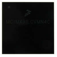
MCIMX31LCVMN4C Freescale Semiconductor, MCIMX31LCVMN4C Datasheet - Page 15

MCIMX31LCVMN4C
Manufacturer Part Number
MCIMX31LCVMN4C
Description
IC MPU MAP I.MX31L 473-MAPBGA
Manufacturer
Freescale Semiconductor
Series
i.MX31r
Specifications of MCIMX31LCVMN4C
Core Processor
ARM11
Core Size
32-Bit
Speed
400MHz
Connectivity
1-Wire, ATA, EBI/EMI, FIR, I²C, MMC/SD, PCMCIA, SIM, SPI, SSI, UART/USART, USB, USB OTG
Peripherals
DMA, LCD, POR, PWM, WDT
Program Memory Type
ROMless
Ram Size
16K x 8
Voltage - Supply (vcc/vdd)
1.22 V ~ 3.3 V
Oscillator Type
External
Operating Temperature
-40°C ~ 85°C
Package / Case
473-MAPBGA
Lead Free Status / RoHS Status
Lead free / RoHS Compliant
Number Of I /o
-
Eeprom Size
-
Program Memory Size
-
Data Converters
-
Available stocks
Company
Part Number
Manufacturer
Quantity
Price
Company:
Part Number:
MCIMX31LCVMN4C
Manufacturer:
Freescale Semiconductor
Quantity:
10 000
Company:
Part Number:
MCIMX31LCVMN4CR2
Manufacturer:
Freescale Semiconductor
Quantity:
10 000
4.2
Any MCIMX31C board design must comply with the power-up and power-down sequence guidelines as
described in this section to guarantee reliable operation of the device. Any deviation from these sequences
may result in any or all of the following situations:
4.2.1
The Power On Reset (POR) pin must be kept asserted (low) throughout the power-up sequence. Power-up
logic must guarantee that all power sources reach their target values prior to the release (de-assertion) of
POR.
Freescale Semiconductor
•
•
•
NVCC2, NVCC21, NVCC22
Figure 2
Cause excessive current during power-up phase
Prevent the device from booting
Cause irreversible damage to the MCIMX31C (worst-case scenario)
Supply Power-Up/Power-Down Requirements and Restrictions
Stages need to be performed in the order shown; however, within each stage,
Powering Up
supplies can be powered up in any order. For example, supplies IOQVDD, NVCC1,
and NVCC3 through NVCC10 do not need to be powered up in the order shown.
NVCC6 and NVCC9 must be at the same voltage potential. These supplies
are connected together on-chip to optimize ESD damage immunity.
and
Figure 2. Option 1 Power-Up Sequence for Silicon Revision 2.0 and 2.0.1
IOQVDD, NVCC1, NVCC3–10
Figure 3
QVCC, QVCC1, QVCC4
Hold POR Asserted
Release POR
1, 3
4
show two options of the power-up sequence.
MCIMX31C/MCIMX31LC Technical Data, Rev. 4.3
FVCC, MVCC, SVCC, UVCC
1
1, 2
CAUTION
NOTE
Notes:
1
2
3
4
5
The board design must guarantee that supplies reach 90% level before
transition to the next state, using Power Management IC or other
means.
The NVCC1 supply must not precede IOQVDD by more than 0.2 V until
IOQVDD has reached 1.5 V. If IOQVDD is powered up first, there are
no restrictions.
The parallel paths in the flow indicate that supply group NVCC2,
NVCC21, and NVCC22, and supply group FVCC, MVCC, SVCC, and
UVCC ramp-ups are independent.
and 2.0.1. This supply is dedicated for fuse burning (programming),
and should not be driven upon boot-up.
Raising IOQVDD before NVCC21 produces a slight increase in current
drain on IOQVDD of approximately 3–5 mA. The current increase will
not damage the IC. Refer to Errata ID TLSbo91750 for details.
FUSE_VDD should not be driven on power-up for Silicon Revision 2.0
1,3
Electrical Characteristics
15


