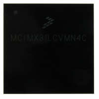
MCIMX31LCVMN4C Freescale Semiconductor, MCIMX31LCVMN4C Datasheet - Page 50

MCIMX31LCVMN4C
Manufacturer Part Number
MCIMX31LCVMN4C
Description
IC MPU MAP I.MX31L 473-MAPBGA
Manufacturer
Freescale Semiconductor
Series
i.MX31r
Specifications of MCIMX31LCVMN4C
Core Processor
ARM11
Core Size
32-Bit
Speed
400MHz
Connectivity
1-Wire, ATA, EBI/EMI, FIR, I²C, MMC/SD, PCMCIA, SIM, SPI, SSI, UART/USART, USB, USB OTG
Peripherals
DMA, LCD, POR, PWM, WDT
Program Memory Type
ROMless
Ram Size
16K x 8
Voltage - Supply (vcc/vdd)
1.22 V ~ 3.3 V
Oscillator Type
External
Operating Temperature
-40°C ~ 85°C
Package / Case
473-MAPBGA
Lead Free Status / RoHS Status
Lead free / RoHS Compliant
Number Of I /o
-
Eeprom Size
-
Program Memory Size
-
Data Converters
-
Available stocks
Company
Part Number
Manufacturer
Quantity
Price
Company:
Part Number:
MCIMX31LCVMN4C
Manufacturer:
Freescale Semiconductor
Quantity:
10 000
Company:
Part Number:
MCIMX31LCVMN4CR2
Manufacturer:
Freescale Semiconductor
Quantity:
10 000
1
2
3
4
Electrical Characteristics
4.3.13
This section describes the electrical information of the I
4.3.13.1 I
Figure 41
supply is 2.7 V. 1
50
IC10
IC11
IC12
IC1
IC2
IC3
IC4
IC5
IC6
IC7
IC8
IC9
A device must internally provide a hold time of at least 300 ns for I2DAT signal in order to bridge the undefined region of the
falling edge of I2CLK.
The maximum hold time has to be met only if the device does not stretch the LOW period (ID IC6) of the I2CLK signal.
A Fast-mode I
250 ns must then be met. This will automatically be the case if the device does not stretch the LOW period of the I2CLK signal.
If such a device does stretch the LOW period of the I2CLK signal, it must output the next data bit to the I2DAT line max_rise_time
(ID No IC10) + data_setup_time (ID No IC8) = 1000 + 250 = 1250 ns (according to the Standard-mode I
before the I2CLK line is released.
C
ID
I2CLK
b
I2DAT
= total capacitance of one bus line in pF.
I2CLK cycle time
Set-up time for STOP condition
HIGH Period of I2CLK Clock
LOW Period of the I2CLK Clock
Data set-up time
Bus free time between a STOP and START condition
Rise time of both I2DAT and I2CLK signals
Fall time of both I2DAT and I2CLK signals
Capacitive load for each bus line (C
Hold time (repeated) START condition
Data hold time
Set-up time for a repeated START condition
depicts the timing of I
I
2
IC2
2
C Electrical Specifications
2
START
C-bus device can be used in a standard-mode I
C Module Timing
Table 40. I
IC10
IC6
Parameter
IC8
2
C Module Timing Parameters—I
IC1
MCIMX31C/MCIMX31LC Technical Data, Rev. 4.3
2
IC10
C module.
Figure 41. I
IC5
b
)
IC4
Table 40
2
IC11
C Bus Timing Diagram
IC11
lists the I
2
C-bus system, but the requirement of set-up time (ID IC7) of
2
C Module.
IC7
Standard Mode
Min
250
2
4.0
4.0
4.0
4.7
4.7
4.7
10
2
0
—
—
—
START
C module timing parameters where the I/O
C Pin I/O Supply=2.7 V
1
3.45
1000
Max
300
400
—
—
—
—
—
—
—
—
2
20+0.1C
20+0.1C
IC3
100
Min
2.5
0.6
0.6
0.6
1.3
0.6
1.3
0
—
STOP
Fast Mode
1
3
Freescale Semiconductor
b
b
4
4
2
C-bus specification)
IC9
Max
0.9
300
300
400
—
—
—
—
—
—
—
—
START
2
Unit
pF
μs
μs
μs
μs
μs
μs
μs
ns
μs
ns
ns


