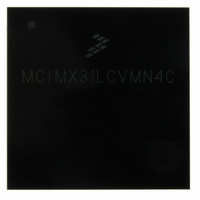
MCIMX31LCVMN4C Freescale Semiconductor, MCIMX31LCVMN4C Datasheet - Page 35

MCIMX31LCVMN4C
Manufacturer Part Number
MCIMX31LCVMN4C
Description
IC MPU MAP I.MX31L 473-MAPBGA
Manufacturer
Freescale Semiconductor
Series
i.MX31r
Specifications of MCIMX31LCVMN4C
Core Processor
ARM11
Core Size
32-Bit
Speed
400MHz
Connectivity
1-Wire, ATA, EBI/EMI, FIR, I²C, MMC/SD, PCMCIA, SIM, SPI, SSI, UART/USART, USB, USB OTG
Peripherals
DMA, LCD, POR, PWM, WDT
Program Memory Type
ROMless
Ram Size
16K x 8
Voltage - Supply (vcc/vdd)
1.22 V ~ 3.3 V
Oscillator Type
External
Operating Temperature
-40°C ~ 85°C
Package / Case
473-MAPBGA
Lead Free Status / RoHS Status
Lead free / RoHS Compliant
Number Of I /o
-
Eeprom Size
-
Program Memory Size
-
Data Converters
-
Available stocks
Company
Part Number
Manufacturer
Quantity
Price
Company:
Part Number:
MCIMX31LCVMN4C
Manufacturer:
Freescale Semiconductor
Quantity:
10 000
Company:
Part Number:
MCIMX31LCVMN4CR2
Manufacturer:
Freescale Semiconductor
Quantity:
10 000
4.3.9.2
All WEIM output control signals may be asserted and deasserted by internal clock related to BCLK rising
edge or falling edge according to corresponding assertion/negation control fields. Address always begins
related to BCLK falling edge but may be ended both on rising and falling edge in muxed mode according
to control register configuration. Output data begins related to BCLK rising edge except in muxed mode
where both rising and falling edge may be used according to control register configuration. Input data,
ECB and DTACK all captured according to BCLK rising edge time.
WEIM module, and
Freescale Semiconductor
Wireless External Interface Module (WEIM)
High is defined as 80% of signal value and low is defined as 20% of signal
value.
Timing for HCLK is 133 MHz and internal NFC clock (flash clock) is
approximately 33 MHz (30 ns). All timings are listed according to this NFC
clock frequency (multiples of NFC clock phases), except NF16 and NF17,
which are not NFC clock related.
Table 30
lists the timing parameters.
MCIMX31C/MCIMX31LC Technical Data, Rev. 4.3
NOTE
NOTE
Figure 26
depicts the timing of the
Electrical Characteristics
35


