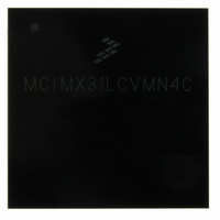
MCIMX31LCVMN4C Freescale Semiconductor, MCIMX31LCVMN4C Datasheet - Page 22

MCIMX31LCVMN4C
Manufacturer Part Number
MCIMX31LCVMN4C
Description
IC MPU MAP I.MX31L 473-MAPBGA
Manufacturer
Freescale Semiconductor
Series
i.MX31r
Specifications of MCIMX31LCVMN4C
Core Processor
ARM11
Core Size
32-Bit
Speed
400MHz
Connectivity
1-Wire, ATA, EBI/EMI, FIR, I²C, MMC/SD, PCMCIA, SIM, SPI, SSI, UART/USART, USB, USB OTG
Peripherals
DMA, LCD, POR, PWM, WDT
Program Memory Type
ROMless
Ram Size
16K x 8
Voltage - Supply (vcc/vdd)
1.22 V ~ 3.3 V
Oscillator Type
External
Operating Temperature
-40°C ~ 85°C
Package / Case
473-MAPBGA
Lead Free Status / RoHS Status
Lead free / RoHS Compliant
Number Of I /o
-
Eeprom Size
-
Program Memory Size
-
Data Converters
-
Available stocks
Company
Part Number
Manufacturer
Quantity
Price
Company:
Part Number:
MCIMX31LCVMN4C
Manufacturer:
Freescale Semiconductor
Quantity:
10 000
Company:
Part Number:
MCIMX31LCVMN4CR2
Manufacturer:
Freescale Semiconductor
Quantity:
10 000
Electrical Characteristics
When bus buffers are used, the ata_data bus buffer is special. This is a bidirectional bus buffer, so a
direction control signal is needed. This direction control signal is ata_buffer_en. When its high, the bus
should drive from host to device. When its low, the bus should drive from device to host. Steering of the
signal is such that contention on the host and device tri-state busses is always avoided.
4.3.5.1
In the timing equations, some timing parameters are used. These parameters depend on the implementation
of the ATA interface on silicon, the bus buffer used, the cable delay and cable skew.
timing parameters.
22
tskew1
tskew2
tskew3
tcable1
tcable2
tskew4
Name
ti_dh
ti_ds
tbuf
tsui
tco
tsu
thi
T
Bus clock period (ipg_clk_ata)
Set-up time ata_data to ata_iordy edge (UDMA-in only)
Hold time ata_iordy edge to ata_data (UDMA-in only)
Propagation delay bus clock L-to-H to
ata_cs0, ata_cs1, ata_da2, ata_da1, ata_da0, ata_dior, ata_diow, ata_dmack, ata_data,
ata_buffer_en
Set-up time ata_data to bus clock L-to-H
Set-up time ata_iordy to bus clock H-to-L
Hold time ata_iordy to bus clock H to L
Max difference in propagation delay bus clock L-to-H to any of following signals
ata_cs0, ata_cs1, ata_da2, ata_da1, ata_da0, ata_dior, ata_diow, ata_dmack, ata_data
(write), ata_buffer_en
Max difference in buffer propagation delay for any of following signals
ata_cs0, ata_cs1, ata_da2, ata_da1, ata_da0, ata_dior, ata_diow, ata_dmack, ata_data
(write), ata_buffer_en
Max difference in buffer propagation delay for any of following signals ata_iordy, ata_data
(read)
Max buffer propagation delay
Cable propagation delay for ata_data
Cable propagation delay for control signals ata_dior, ata_diow, ata_iordy, ata_dmack
Max difference in cable propagation delay between ata_iordy and ata_data (read)
Timing Parameters
MCIMX31C/MCIMX31LC Technical Data, Rev. 4.3
Table 21. ATA Timing Parameters
Description
UDMA0, UDMA1, UDMA2, UDMA3, UDMA4
UDMA2, UDMA3
UDMA0
UDMA1
UDMA4
UDMA5
UDMA5
Table 21
Freescale Semiconductor
Contributing Factor
peripheral clock
transceiver
transceiver
transceiver
frequency
12.0 ns
Value/
5.0 ns
4.6 ns
8.5 ns
8.5 ns
2.5 ns
15 ns
10 ns
shows ATA
cable
cable
cable
7 ns
5 ns
4 ns
7 ns
1


